Chat
Welcome to Flux
Treat Flux like your intern. Tell it what you'd like to build and it'll get to work. You can also ask it questions, brainstorm ideas, and teach it your preferences. Learn More
Explain project
Write a project description
Find schematic issues
Create a test plan
Simulate a circuit
Prepare for Manufacturing
Component Selection Workflow
New Subsystem Wizard
Operating conditions
Part Specifications
Verify Part Details
Recommend similar parts
Ready.
New Comment
Someone is typing...
2
create a high level mermaid block diagram of this project. Include key component...
1y
Sure, I'll create a high-level Mermaid block diagram for your project. Each block will represent a key component of the circuit, and I'll include the manufacturer part number where applicable.
Here's how it looks in Mermaid syntax:
Diagram
In this diagram:
- The central component is the STM8S003F3P microcontroller from STMicroelectronics.
- Power Supply is connected to the VDD pin of the microcontroller.
- A Capacitor is connected to the VCAP pin of the microcontroller.
- Various I/O ports are grouped under an IO_Ports subgraph, showing their connections to specific pins of the microcontroller.
- NRST and VSS pins are also highlighted for clarity.
You can visualize this diagram in a Mermaid-compatible viewer to see the blocks clearly.
1y
Someone is typing...
5
how do I use Flux?
i added this stm controller please add all the necessary components on the vcc of it
1y
1y
Using Flux.ai for designing electronic schematics and PCB layouts is a streamlined process. Here's a helpful guide to get you started:
1. Create an Account
- Visit Flux signup to register for an account. You can sign up using your email and password or link your Google account.
- Canvas: The central workspace where you'll create schematics and PCB layouts.
- Library: Contains components that you can drag and drop onto the canvas.
- Inspector: Allows you to modify properties of selected components.
- Toolbar: Provides tools for creating and editing your design.
- Drag components from the library onto the canvas.
- Position them as needed. You can rotate and move components to fit your design requirements.
- Use wires to connect component pins according to your schematic.
- Simply click on a pin and drag the wire to the destination pin.
- Switch to PCB layout mode to arrange components on a board.
- Route traces between component pads.
- Flux also offers simulation tools to test your circuit. Look at the tutorial for more information on how simulations run inside Flux.
- For support, you can join the Flux Slack community to ask questions and meet other users.
- Flux also offers a range of video tutorials and crash courses available on YouTube.
- When Copilot suggests specific connections on your schematic, use the "Take Action" button to apply those connections.
Would you like more details on any specific aspect of using Flux?
1y
Someone is typing...
4
PD1
PC3
PD4
VDD
PC5
PC4
PB4
PB5
PD2
PC7
VSS
PC6
NRST
PA3
PA1
PD5
PA2
PD6
VCAP
PD3
Reviews

- Wirelessly connects nets on schematic. Used to organize schematics and separate functional blocks. To wirelessly connect net portals, give them same designator. #portaljharwinbarrozo43.0M
- Wirelessly connects power nets on schematic. Identical to the net portal, but with a power symbol. Used to organize schematics and separate functional blocks. To wirelessly connect power net portals, give them the same designator. #portal #powerjharwinbarrozo11.4M
- A generic fixed resistor for rapid developing circuit topology. Save precious design time by seamlessly add more information to this part (value, footprint, etc.) as it becomes available. Standard resistor values: 1.0Ω 10Ω 100Ω 1.0kΩ 10kΩ 100kΩ 1.0MΩ 1.1Ω 11Ω 110Ω 1.1kΩ 11kΩ 110kΩ 1.1MΩ 1.2Ω 12Ω 120Ω 1.2kΩ 12kΩ 120kΩ 1.2MΩ 1.3Ω 13Ω 130Ω 1.3kΩ 13kΩ 130kΩ 1.3MΩ 1.5Ω 15Ω 150Ω 1.5kΩ 15kΩ 150kΩ 1.5MΩ 1.6Ω 16Ω 160Ω 1.6kΩ 16kΩ 160kΩ 1.6MΩ 1.8Ω 18Ω 180Ω 1.8KΩ 18kΩ 180kΩ 1.8MΩ 2.0Ω 20Ω 200Ω 2.0kΩ 20kΩ 200kΩ 2.0MΩ 2.2Ω 22Ω 220Ω 2.2kΩ 22kΩ 220kΩ 2.2MΩ 2.4Ω 24Ω 240Ω 2.4kΩ 24kΩ 240kΩ 2.4MΩ 2.7Ω 27Ω 270Ω 2.7kΩ 27kΩ 270kΩ 2.7MΩ 3.0Ω 30Ω 300Ω 3.0KΩ 30KΩ 300KΩ 3.0MΩ 3.3Ω 33Ω 330Ω 3.3kΩ 33kΩ 330kΩ 3.3MΩ 3.6Ω 36Ω 360Ω 3.6kΩ 36kΩ 360kΩ 3.6MΩ 3.9Ω 39Ω 390Ω 3.9kΩ 39kΩ 390kΩ 3.9MΩ 4.3Ω 43Ω 430Ω 4.3kΩ 43KΩ 430KΩ 4.3MΩ 4.7Ω 47Ω 470Ω 4.7kΩ 47kΩ 470kΩ 4.7MΩ 5.1Ω 51Ω 510Ω 5.1kΩ 51kΩ 510kΩ 5.1MΩ 5.6Ω 56Ω 560Ω 5.6kΩ 56kΩ 560kΩ 5.6MΩ 6.2Ω 62Ω 620Ω 6.2kΩ 62KΩ 620KΩ 6.2MΩ 6.8Ω 68Ω 680Ω 6.8kΩ 68kΩ 680kΩ 6.8MΩ 7.5Ω 75Ω 750Ω 7.5kΩ 75kΩ 750kΩ 7.5MΩ 8.2Ω 82Ω 820Ω 8.2kΩ 82kΩ 820kΩ 8.2MΩ 9.1Ω 91Ω 910Ω 9.1kΩ 91kΩ 910kΩ 9.1MΩ #generics #CommonPartsLibraryjharwinbarrozo1.5M
- A generic fixed capacitor ideal for rapid circuit topology development. You can choose between polarized and non-polarized types, its symbol and the footprint will automatically adapt based on your selection. Supported options include standard SMD sizes for ceramic capacitors (e.g., 0402, 0603, 0805), SMD sizes for aluminum electrolytic capacitors, and through-hole footprints for polarized capacitors. Save precious design time by seamlessly add more information to this part (value, footprint, etc.) as it becomes available. Standard capacitor values: 1.0pF 10pF 100pF 1000pF 0.01uF 0.1uF 1.0uF 10uF 100uF 1000uF 10,000uF 1.1pF 11pF 110pF 1100pF 1.2pF 12pF 120pF 1200pF 1.3pF 13pF 130pF 1300pF 1.5pF 15pF 150pF 1500pF 0.015uF 0.15uF 1.5uF 15uF 150uF 1500uF 1.6pF 16pF 160pF 1600pF 1.8pF 18pF 180pF 1800pF 2.0pF 20pF 200pF 2000pF 2.2pF 22pF 20pF 2200pF 0.022uF 0.22uF 2.2uF 22uF 220uF 2200uF 2.4pF 24pF 240pF 2400pF 2.7pF 27pF 270pF 2700pF 3.0pF 30pF 300pF 3000pF 3.3pF 33pF 330pF 3300pF 0.033uF 0.33uF 3.3uF 33uF 330uF 3300uF 3.6pF 36pF 360pF 3600pF 3.9pF 39pF 390pF 3900pF 4.3pF 43pF 430pF 4300pF 4.7pF 47pF 470pF 4700pF 0.047uF 0.47uF 4.7uF 47uF 470uF 4700uF 5.1pF 51pF 510pF 5100pF 5.6pF 56pF 560pF 5600pF 6.2pF 62pF 620pF 6200pF 6.8pF 68pF 680pF 6800pF 0.068uF 0.68uF 6.8uF 68uF 680uF 6800uF 7.5pF 75pF 750pF 7500pF 8.2pF 82pF 820pF 8200pF 9.1pF 91pF 910pF 9100pF #generics #CommonPartsLibraryjharwinbarrozo1.5M
- A generic fixed inductor for rapid developing circuit topology. *You can now change the footprint and 3D model at the top level anytime you want. This is the power of #genericsjharwinbarrozo15.5k
- An electrical connector acting as reusable interface to a conductor and creating a point where external circuits can be connected.Terminal
- 47 kOhms ±5% 0.125W, 1/8W Chip Resistor 0805 (2012 Metric) Automotive AEC-Q200 Thick Film #forLedBlinkjharwinbarrozo1.2M
- 10uF Capacitor Aluminum Polymer 20% 16V SMD 5x5.3mm #forLedBlink #commonpartslibrary #capacitor #aluminumpolymer #radialcanjharwinbarrozo1.2M
- Yellow 595nm LED Indication - Discrete 1.7V 1206 (3216 Metric) #forLedBlinkjharwinbarrozo1.1M


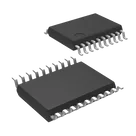
STM8 STM8S Microcontroller IC 8-Bit 16MHz 8KB (8K x 8) FLASH 20-TSSOP #microcontrollers #stm8
#commonpartslibrary
Pricing & Availability
Distributor | Qty 1 |
|---|
Assets
kicad_mod
TSSOP-20_4.4x6.5mm_P0.65mm-FS.kicad_mod
TSSOP-20_4.4x6.5mm_P0.65mm-FS
TSSOP-20_4.4x6.5mm_P0.65mm-removebg-preview.png
TSSOP-20_4.4x6.5mm_P0.65mm-removebg-previewThumbnailTSSOP-20_4.4x6.5mm_P0.65mm-3D.step
3D3D ModelControls
Welcome 👋
Flux accelerates your PCB design with AI.
Create your account to start using this component and bring your ideas to life.
oguzz
copilot
oguzz
copilot