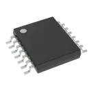
Sure, these are the terminals of the MAX31856 Precision Thermocouple to Digital Converter with Linearization by Maxim Integrated. Here's a brief overview:
T- (Pin 3): This is the negative input of the thermocouple.
T+ (Pin 4): This is the positive input of the thermocouple.
~DRDY (Pin 7): This stands for "Data Ready". It's an output pin that goes low when a new temperature reading is available from the device. This can be very handy for interrupt-driven designs.
BIAS (Pin 2): This is the bias current terminal. It is tied to an internal current source in the chip.
DNC (Pin 6): This stands for "Do Not Connect". As the name implies, no connection should be made to this pin.
DGND (Pin 14): This stands for "Digital Ground". It's the ground return path for the digital portion of the circuit.
AVDD (Pin 5): This stands for "Analog Power". It's the power supply for the analog parts of the IC. Typically, this should be a clean and noise-free power supply.
DVDD (Pin 8): This stands for "Digital Power". It's the power supply for the digital parts of the IC.
SDO (Pin 11): This stands for "Serial Data Out". It's the Data output of the SPI interface.
AGND (Pin 1): This stands for "Analog Ground". It's the ground return path for the analog portion of the circuit.
~CS (Pin 9): This stands for "Chip Select". It's an active-low signal that begins an SPI transaction when pulled low.
~FAULT (Pin 13): This is an active-low fault output. It goes low if the device detects a fault condition.
SDI (Pin 12): This stands for "Serial Data In". It is the Data input of the SPI interface.
SCK (Pin 10): This stands for "Serial Clock". It provides the timing for the data bits in the SPI interface.
Note: The "~" symbol represents the negation. When it's in front of a signal (like ~CS, ~DRDY, and ~FAULT), it indicates that the signal is active low. i.e., a '0' operates the function and a '1' shuts the function off.
freeflyfreak
freeflyfreak
copilot