Switches
A switch is a device that allows electricity to flow through a circuit by completing or interrupting the connection. It is a common component in electrical and electronic systems and is used in a variety of applications, such as controlling the flow of electricity in a circuit, turning devices on and off, and routing electrical signals. One of the primary use cases for switches is to control the flow of electricity in a circuit. This can be done by manually flipping the switch or by using a control mechanism, such as a timer or a sensor. Another common use for switches is to turn devices on and off. This can be done using a switch that is built into the device or by using a separate switch that is connected to the device. In addition to these basic use cases, switches can also be used to route electrical signals. For example, a switch can be used to route a signal from one device to another or to direct a signal to a specific circuit or component. If you're looking for a wide variety of switches for your projects, flux.ai has the world's largest community-driven public library of them. The library includes footprints, symbols, datasheets, and simulation models for a wide range of switches, making it easy to find the right switch for your needs.
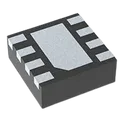
TPS62172DSGT
Buck Switching Regulator IC Positive Fixed 3.3V 1 Output 500mA 8-WFDFN Exposed Pad The TPS6217x device family are easy to use synchronous step-down DC-DC converters optimized for applications with high power density. A high switching frequency of typically 2.25 MHz allows the use of small inductors and provides fast transient response as well as high output voltage accuracy by utilization of the DCS-Control™ topology. With its wide operating input voltage range of 3 V to 17 V, the devices are ideally suited for systems powered from either a Li-Ion or other battery as well as from 12-V intermediate power rails. It supports up to 0.5-A continuous output current at output voltages between 0.9 V and 6 V (with 100% duty cycle mode). Power sequencing is also possible by configuring the enable and open-drain power good pins. In power save mode, the devices show quiescent current of about 17 μA from VIN. Power save mode, entered automatically and seamlessly if the load is small, maintains high efficiency over the entire load range. In shutdown mode, the device is turned off and shutdown current consumption is less than 2 μA. The device, available in adjustable and fixed output voltage versions, is packaged in a 2-mm × 2-mm 8- pin WSON package (DSG). • DCS-Control™ Topology • Input Voltage Range from 3 V to 17 V • Up to 500-mA Output Current • Adjustable Output Voltage from 0.9 V to 6 V • Fixed Output Voltage Versions • Seamless Power Save Mode Transition • Typically 17-µA Quiescent Current • Power Good Output • 100% Duty Cycle Mode • Short Circuit Protection • Over Temperature Protection • Pin to Pin Compatible with TPS62160 and TPS62125 • Available in a 2-mm × 2-mm 8-Pin WSON Package • Create a Custom Design using the TPS62170 with the WEBENCH® Power Designer #CommonPartsLibrary #IntegratedCircuit #PowerManagement
72 Uses0 StarsSS54
DIODE SCHOTTKY 40V SMA(DO-214AC) The SS54 is a surface-mount Schottky barrier rectifier diode commonly used in power management and protection circuits. It is designed for high-speed switching applications and offers low forward voltage drop for improved efficiency in low-voltage systems. The device is widely used in DC-DC converters, reverse polarity protection, freewheeling circuits, and switching power supplies. Key Features Schottky barrier rectifier technology Maximum reverse voltage: 40 V Average forward current: 5 A Low forward voltage drop (typically around 0.55 V) High surge current capability Fast switching speed Surface-mount package (commonly DO-214AB / SMC) Low power loss and high efficiency Suitable for high-frequency applications Guard ring protection for improved reliability RoHS compliant versions available from many manufacturers Typical Applications Switching power supplies DC-DC buck or boost converters Reverse polarity protection Freewheeling / flyback diode applications Battery-powered devices LED drivers Power OR-ing circuits #CommonPartsLibrary #Diode
642 Uses0 StarsAO3401
MOSFET P-CH 30V 4.1A SOT-23 The AO3401 is a 30 V P-Channel Enhancement Mode MOSFET designed for high-efficiency power switching applications. It uses advanced trench MOSFET technology to achieve low on-resistance (RDS(on)), low gate charge, and fast switching performance. Packaged in a compact SOT-23 package, it is widely used in load switching, battery-powered devices, reverse-polarity protection circuits, and power management applications. Key Features P-Channel MOSFET Drain-Source Voltage (VDS): −30 V Continuous Drain Current (ID): up to −4 A (25°C) Low RDS(on): 50 mΩ max @ VGS = −10 V 60 mΩ max @ VGS = −4.5 V 85 mΩ max @ VGS = −2.5 V Low Gate Charge: 7 nC typical @ 4.5 V Gate-Source Voltage Rating: ±12 V Low Threshold Voltage: −0.5 V to −1.3 V Fast Switching Characteristics Compact SOT-23 Surface-Mount Package Operating Junction Temperature: up to 150°C Suitable for Low-Voltage Logic-Level Drive Applications Typical Applications Load switches Battery protection circuits Reverse-polarity protection Power-path management DC-DC converters Portable and battery-powered electronics PWM switching applications #CommonPartsLibrary #Transistor #FET #Mosfet
63 Uses0 StarsTPS62840DLCR
1.8V to 6.5V, 750mA, 60nA IQ step-down converter The TPS62840 is a high-efficiency step-down converter with ultra-low operating quiescent current of typically 60 nA. The device contains special circuitry to achieve just 120 nA IQ in 100% mode to further extend battery life near the end of discharge. The device uses DCS-Control to cleanly power radios and operates with a typical switching frequency of 1.8 MHz. In Power-Save Mode, the device extends the light load efficiency down to a load current range of 1 μA and below. 16 predefined output voltages can be selected by connecting a resistor to pin VSET, making the device flexible for various applications with a minimum amount of external components. The STOP pin of the device immediately eliminates any switching noise in order to take a noise-free measurement in test and measurement systems. The TPS62840 provides an output current of up to 750 mA. With an input voltage of 1.8 V to 6.5 V, the device supports multiple power sources such as 2S to 4S Alkaline, 1S to 2S Li-MnO2 , or 1S Li-Ion/LiSOCl2 • 60-nA operating quiescent current • 100% duty-cycle mode with 120-nA IQ • Input voltage range VIN from 1.8 V to 6.5 V • Output current up to 750 mA • RF friendly DCS-Control™ • 80% efficiency at 1 µA IOUT (3.6 VIN to 1.8 VOUT) • 16 selectable output voltages via VSET pin • Auto transition PFM/PWM or forced-PWM mode • Selectable forced PWM and STOP modes • Output discharge function • 25-nA shutdown current • SON-8, WCSP-6 and thermally enhanced HVSSOP-8 packages #CommonPartsLibrary #IntegratedCircuit #PowerManagement
1.0k Uses0 Stars