Oscillators
ADC09SJ1300AAVT
Analog to Digital Converters - ADC Single-channel, 9-bit, 1.3-GSPS analog-to-digital converter (ADC) with JESD204C interface 144-FCBGA -40 to 85 ADC09xJ1300 is a family of quad, dual and single channel, 9-bit, 1.3GSPS analog-to-digital converters (ADC). Low power consumption, high sampling rate and 9-bit resolution makes the ADC09xJ1300 ideally suited for suited for a variety of multi-channel communications and test systems. Full-power input bandwidth (-3dB) of 6GHz enables direct RF sampling of L-band and S-band. A number of clocking features are included to relax system hardware requirements, such as an internal phase-locked loop (PLL) with integrated voltagecontrolled oscillator (VCO) to generate the sampling clock. Four clock outputs are provided to clock the logic and SerDes of the FPGA or ASIC. A timestamp input and output is provided for pulsed systems. JESD204C serialized interface decreases system size by reducing the amount of printed circuit board (PCB) routing. Interface modes support from 2 to 8 lanes (dual and quad channel devices) or 1 to 4 lanes (for the single channel device), with SerDes baud-rates up to 17.16Gbps, to allow the optimal configuration for each application. Features • ADC Core: – Resolution: 9 Bit – Maximum sampling rate: 1.3GSPS – Non-interleaved architecture – Internal dither reduces high-order harmonics • Performance specifications (–1dBFS): – SNR (100 MHz): 53.5dBFS – ENOB (100 MHz): 8.5 Bits – SFDR (100 MHz): 64dBc – Noise floor (–20dBFS): –143dBFS • Full-scale input voltage: 80 mVPP-DIFF • Full-power input bandwidth: 6GHz • JESD204C Serial data interface: – Support for 2 to 8 (Quad/Dual channel) or 1 to 4 (Single channel) total SerDes lanes – Maximum baud-rate: 17.16Gbps – 64B/66B and 8B/10B encoding modes – Subclass-1 support for deterministic latency – Compatible with JESD204B receivers • Optional internal sampling clock generation – Internal PLL and VCO (7.2–8.2GHz) • SYSREF Windowing eases synchronization • Four clock outputs simplify system clocking – Reference clocks for FPGA or adjacent ADC – Reference clock for SerDes transceivers • Timestamp input and output for pulsed systems • Power consumption (1GSPS): – Quad Channel: 450mW / channel – Dual channel: 625mW / channel – Single channel: 940mW • Power supplies: 1.1V, 1.9V #CommonPartsLibrary #IntegratedCircuit #ADC #HighSpeedADC #RFADC #JESD204C #13GSPS #9bitADC #DirectRFSampling #TexasInstruments #MixedSignal #DataAcquisition #JESD204
0 Uses
0 Stars
RFFC5072
The RFFC5072 is a highly integrated wideband RF frequency conversion IC that combines a fractional-N PLL synthesizer, low phase-noise VCO, and a high-linearity RF mixer in a single device. It is designed for wireless infrastructure, software-defined radio (SDR), test equipment, military communications, and broadband frequency conversion applications. The device can generate local oscillator (LO) frequencies from 85 MHz to 4.2 GHz and perform frequency conversion for RF signals up to 6 GHz while maintaining excellent phase noise and spurious performance. Features 85MHz to 4200MHz LO Frequency Range Fractional-N Synthesizer with Very Low Spurious Levels Typical Step Size 1.5Hz Fully Integrated Low Phase Noise VCO and LO Buffers Integrated Phase Noise • 0.18° rms at 1GHz • 0.50° rms at 3GHz High Linearity RF Mixer(s) 30MHz to 6000MHz Mixer Frequency Range Input IP3 +23dBm Mixer Bias Adjustable for Low Power Operation Full Duplex Mode (RFFC5071) 2.7V to 3.3V Power Supply Low Current Consumption 3- or 4-Wire Serial Interface Applications Wideband Radios Distributed Antenna Systems Diversity Receivers Software Defined Radios Frequency Band Shifters Point-to-Point Radios WiMax/LTE Infrastructure Satellite Communications Wideband Jammers #RFFC5072 #Qorvo #RFMixer #FrequencySynthesizer #PLL #VCO #WidebandRF #FrequencyConverter #SDR #WirelessInfrastructure #RFDesign #MicrowaveEngineering #Telecommunications #EmbeddedSystems #ElectronicsDesign #RFIC #SignalProcessing #HardwareEngineering
0 Uses
0 Stars
RK809-5
QFN-68-EP(7x7) Power Management - Specialized RoHS The RK809-5 is a highly integrated Power Management Integrated Circuit (PMIC) from Rockchip designed for multi-core processor systems and embedded applications. It provides a complete power management solution by integrating multiple high-efficiency DC-DC buck converters, LDO regulators, power sequencing logic, battery fuel gauging, RTC functionality, and audio codec capabilities into a single device. The RK809-5 is commonly used alongside Rockchip SoCs in single-board computers, tablets, AIoT devices, and industrial embedded systems. Key Features Five high-efficiency synchronous buck converters with fast transient response. Nine low-dropout (LDO) voltage regulators for powering sensitive analog and digital circuits. Integrated battery fuel gauge for battery capacity monitoring. Configurable power-up and power-down sequencing (OTP programmable). Dynamic Voltage Scaling (DVS/DVFS) support via I²C interface. Integrated Real-Time Clock (RTC) with 32.768 kHz crystal oscillator support. Two integrated load switches for peripheral power control. Over-current, over-voltage, and thermal protection features. Built-in audio CODEC with headphone driver and Class-D amplifier support. Designed to minimize external component count and simplify power system design. QFN-68-EP (7 mm × 7 mm) package. #RK8095 #RK809 #Rockchip #PMIC #PowerManagementIC #BatteryManagement #AudioCodec #RTC #DVFS #EmbeddedSystems #SingleBoardComputer #IoT #IndustrialElectronics #PowerSupplyDesign #ElectronicsEngineering
1 Use
0 Stars
XL6007E1
The XL6007 regulator is a wide input range, current mode, DC/DC converter which is capable of generating either positive or negative output voltages. It can be configured as either a boost, flyback, SEPIC or inverting converter. The XL6007 built in N-channel power MOSFET and fixed frequency oscillator, current-mode architecture results in stable operation over a wide range of supply and output voltages. The XL6007 regulator is special design for portable electronic equipment. Wide 3.6V to 24V Input Voltage Range Positive or Negative Output Voltage Programming with a Single Feedback Pin Current Mode Control Provides Excellent Transient Response 1.25V reference adjustable version Fixed 400KHz Switching Frequency Maximum 2A Switching Current SW PIN Built in Over Voltage Protection Excellent line and load regulation EN PIN TTL shutdown capability Internal Optimize Power MOSFET High efficiency up to 90% Built in Frequency Compensation Built in Soft-Start Function Built in Thermal Shutdown Function Built in Current Limit Function Available in SOP8 package Applications Automotive and Industrial Boost / Buck-Boost / Inverting Converters Portable Electronic Equipment #commonpartslibrary #integratedcircuit
0 Uses
0 Stars
ADS1293CISQ/NOPB
3 Channel AFE 24 Bit 28-WQFN (5x5) ADS1293CISQ/NOPB is a highly integrated, low-power 3-channel ECG Analog Front-End (AFE) from Texas Instruments. It is designed for portable and battery-powered medical devices, fitness monitors, heart-rate monitoring systems, Holter monitors, and other electrocardiogram (ECG) applications. The device integrates signal acquisition, filtering, lead-off detection, right-leg drive generation, and high-resolution analog-to-digital conversion into a single IC, reducing external component count and system cost. Key Features Three high-resolution ECG acquisition channels 24-bit analog-to-digital conversion Simultaneous pace detection support Ultra-low power consumption of approximately 0.3 mW per channel Low input-referred noise of 7 µVpp (40 Hz bandwidth) Programmable sample rates up to 25.6 ksps Differential input voltage range of ±400 mV Integrated EMI-hardened input filters Flexible input routing matrix Built-in Right-Leg Drive (RLD) amplifier AC and DC lead-off detection Integrated Wilson and Goldberger terminal generation Battery voltage monitoring capability Internal oscillator and voltage reference ALARMB pin for interrupt-driven diagnostics and fault reporting Multiple power-down and standby modes for battery-powered systems SPI-compatible digital interface Operating temperature range: –20°C to +85°C 28-pin WQFN package (5 mm × 5 mm) Typical Applications Portable 1-, 3-, 5-, 6-, 7-, 8-, and 12-lead ECG systems Holter monitors Event recorders Telemedicine devices Patient vital-sign monitoring equipment Automated External Defibrillators (AEDs) Sports and fitness heart-rate monitors Wearable medical devices Hashtags #commonpartslibrary #integratedcircuit #TexasInstruments #ADS1293 #AFE #AnalogFrontEnd #ECG #Electrocardiogram #MedicalElectronics #HealthTech #WearableDevices #HeartRateMonitor #PatientMonitoring #BiomedicalEngineering #24BitADC #LowPowerDesign #SPI #SignalConditioning #PortableMedicalDevices #HolterMonitor #Telemedicine #VitalSignsMonitoring #EmbeddedSystems #MixedSignalIC #WQFN28 #BatteryPoweredDevices #MedicalInstrumentation
0 Uses
0 Stars
PCA9450CHNY
Power Management IC for iMX8M 5V 6A 6 Buck + 5 LDO The PCA9450CHNY is a highly integrated Power Management Integrated Circuit (PMIC) from NXP Semiconductors, specifically designed to power the i.MX 8M family of application processors, particularly the i.MX 8M Plus. It integrates multiple high-efficiency DC-DC buck converters, LDO regulators, power sequencing logic, load switching, voltage monitoring, and system control functions into a single device. The PCA9450C variant features a configurable dual-phase 6 A buck regulator for powering high-current processor cores while supporting Dynamic Voltage Scaling (DVS) for optimized power efficiency. Key Features Six high-efficiency switching regulators (Buck converters) PCA9450C variant supports a configurable 6 A dual-phase buck regulator Three 3 A buck regulators with Dynamic Voltage Scaling (DVS) Remote-sense capability on major buck outputs for IR-drop compensation Five integrated LDO regulators Supports DDR4, LPDDR4, and DDR3L memory configurations 400 mA load switch with active discharge Dual-channel logic level translator Integrated 32.768 kHz crystal oscillator driver Fast-mode Plus (Fm+) 1 MHz I²C interface Programmable power sequencing and voltage control Power ON/OFF and Standby/Run mode control inputs Protection features including UVLO, thermal shutdown, fault monitoring, and soft-start Operating temperature range: −40°C to +105°C 56-pin HVQFN package (7 mm × 7 mm, 0.4 mm pitch) Optimized for i.MX 8M Mini, Nano, and Plus processors, especially the i.MX 8M Plus for the PCA9450C variant. #CommonPartsLibrary #PCA9450CHNY #PCA9450C #NXP #PMIC #PowerManagementIC #PowerSupply #VoltageRegulator #BuckConverter #LDO #DynamicVoltageScaling #DVS #IMX8M #IMX8MPlus #EmbeddedSystems #IndustrialElectronics #PowerManagement #HVQFN56 #Semiconductor #IntegratedCircuit #IC #CommonPartsLibrary #ElectronicsDesign #HardwareDesign #PCBDesign #EmbeddedLinux #IoT #ProcessorPowerManagement #PowerSequencing #SystemPower #NXPSemiconductors
0 Uses
0 Stars
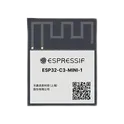
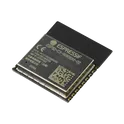
ESP32-C3-WROOM-02-N4
20.5dBm ESP32-C3 Chip 2.4GHz VFQFN-32-EP WiFi Modules ROHS RF Transceiver ICs ESP32-C3-WROOM-02-N4 BULETM-SMD_ESPRESSIF_ESP32-C3-WROOM-02-N4-4MB LCSC Part Number: C2934560 Espressif ESP32-C3-WROOM-02 wireless MCU module, based on ESP32-C3 32-bit RISC-V single-core processor up to 160MHz, supports 2.4GHz Wi-Fi 802.11b/g/n and Bluetooth LE 5.0 with Bluetooth mesh, 4MB or 8MB SPI flash options, 384KB ROM, 400KB SRAM and 8KB RTC SRAM, up to 15 GPIOs, SPI, UART, I2C, I2S, LED PWM, USB Serial/JTAG, ADC, timers and watchdogs, integrated 40MHz crystal oscillator, 3.0V to 3.6V supply voltage, on-board PCB antenna, RoHS/REACH compliant, 18.0 x 20.0 x 3.2mm module size. Search Keywords: ESP32-C3-WROOM-02, ESP32-C3-WROOM-02-N4, ESP32-C3-WROOM-02-H4, ESP32-C3-WROOM-02-N8, Espressif ESP32-C3-WROOM-02, ESP32-C3 WiFi Bluetooth module, ESP32-C3 RISC-V module, WiFi BLE 5 module, 802.11bgn module, Bluetooth mesh module, ESP32-C3 PCB antenna module, ESP32-C3 4MB flash module, ESP32-C3 8MB flash module Hashtags: #ESP32C3WROOM02 #ESP32C3WROOM02N4 #ESP32C3WROOM02H4 #ESP32C3WROOM02N8 #EspressifESP32C3 #ESP32C3 #WiFiBluetoothModule #WiFiModule #BluetoothLEModule #BLE5Module #RISCVMCU #IoTModule #PCBantenna #80211bgn
89 Uses
0 Stars
ASTX-H12-25.000MHZ-T
25 MHz TCXO HCMOS Oscillator 3.3V Enable/Disable 4-SMD, No Lead ASTX-H12 25.000 MHz Abracon ASTX-H12 HCMOS output SMD TCXO, 2.5 x 2.0 x 0.9mm package, 3.2MHz to 55MHz frequency range, standard frequencies 5MHz to 44MHz, 3.3V typical supply voltage, frequency stability up to ±2.5ppm over temperature, ±2.0ppm tolerance at 25°C, low current consumption, 15pF load, 5ns max rise/fall time, tri-state standby function, MSL-1, RoHS/RoHS II compliant, suitable for cellular phones, wireless modules, GPS, RF communication and precision clock reference applications. Search Keywords: ASTX-H12, Abracon ASTX-H12, ASTX-H12 TCXO, HCMOS TCXO, SMD TCXO 2.5x2.0mm, 3.3V TCXO, 26MHz TCXO, 40MHz TCXO, 3.2MHz to 55MHz TCXO, low power TCXO, precision clock oscillator, RF reference oscillator, GPS TCXO, wireless module TCXO, ASTX-H12 datasheet Hashtags: #ASTXH12 #AbraconASTXH12 #TCXO #HCMOSTCXO #SMDOscillator #CrystalOscillator #TemperatureCompensatedOscillator #33VTCXO #25x20mmOscillator #PrecisionClock #FrequencyReference #RFOscillator #GPSOscillator #WirelessClock
0 Uses
0 Stars
ADF4351BCPZ
Clock Generators, PLLs, Frequency Synthesizers ADF4351BCPZ LFCSP-32_L5.0-W5.0-P0.50-BL-EP3.5 LCSC Part Number: C654681 JLCPCB Part Class: Extended Part Manufactured by ADI(亚德诺)/LINEAR(凌特) Analog Devices ADF4351 wideband fractional-N and integer-N PLL frequency synthesizer with integrated voltage-controlled oscillator (VCO), generating RF output frequencies from 35MHz to 4.4GHz. Features low phase noise, programmable output divider ratios (/1, /2, /4, /8, /16, /32, /64), programmable RF output power, dual-modulus prescaler (4/5 or 8/9), analog and digital lock detect, fast lock mode, cycle slip reduction, auxiliary RF output, RF mute function, and 3-wire serial programming interface. Operates from 3.0V to 3.6V and is widely used in RF signal generators, local oscillators, SDR systems, wireless infrastructure, test equipment, microwave communications, clock generation, and laboratory instrumentation. Search Keywords: ADF4351, Analog Devices ADF4351, ADF4351BRUZ, RF synthesizer, PLL synthesizer, fractional N PLL, integer N PLL, integrated VCO, 35MHz to 4.4GHz synthesizer, RF signal generator IC, microwave frequency synthesizer, local oscillator PLL, SDR synthesizer, programmable RF generator, low phase noise synthesizer, SPI PLL synthesizer, RF clock generator Hashtags: #ADF4351 #AnalogDevices #PLL #FractionalNPLL #IntegerNPLL #FrequencySynthesizer #RFSynthesizer #IntegratedVCO #RFGenerator #SignalGenerator #LocalOscillator #MicrowaveRF #SDR #ClockGenerator #RFIC #WirelessInfrastructure #TestEquipment #LowPhaseNoise #SPIInterface #ADF4351Module
29 Uses
0 Stars
ATTINY1616-MFR
ATTINY1616-MFR QFN-20_L3.0-W3.0-P0.40-TL-EP1.7 LCSC Part Number: C1338523 JLCPCB Part Class: Extended Part Manufactured by MICROCHIP(美国微芯) Microchip ATtiny1614/1616/1617 tinyAVR 1-series 8-bit microcontroller, AVR CPU running up to 20MHz, up to 16KB self-programmable Flash memory, 256B EEPROM and 2KB SRAM, 1.8V to 5.5V operating voltage range, single-pin UPDI programming and debug interface, power-on reset and brown-out detector, internal 16/20MHz oscillator, timers, watchdog, USART, SPI, I2C/TWI, 10-bit ADC, DAC, analog comparators, event system, configurable custom logic and peripheral touch controller, available in 14-pin, 20-pin and 24-pin packages depending on variant. Search Keywords: ATtiny1614, ATtiny1616, ATtiny1617, Microchip ATtiny1614, Microchip ATtiny1616, Microchip ATtiny1617, tinyAVR 1-series, AVR 8-bit microcontroller, ATtiny 16KB Flash, ATtiny UPDI, ATtiny1616 microcontroller, ATtiny1617 MCU, ATtiny1614 MCU, 20MHz AVR microcontroller, ATtiny I2C SPI USART, ATtiny1616 datasheet, ATtiny1614 datasheet, ATtiny1617 datasheet Hashtags: #ATtiny1614 #ATtiny1616 #ATtiny1617 #MicrochipATtiny #MicrochipMCU #tinyAVR #tinyAVR1Series #AVRMicrocontroller #8bitMicrocontroller #ATtinyMCU #UPDI #16KBFlashMCU #20MHzMCU #I2CMCU #SPIMCU #USARTMCU #ADCmicrocontroller #TouchControllerMCU
27 Uses
0 Stars
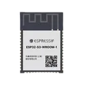
ESP32-S3-WROOM-1-N8
ESP32-S3-WROOM-1-N8 is a high-performance Wi-Fi and Bluetooth Low Energy (BLE) module from Espressif Systems. It is built around the ESP32-S3 SoC, featuring a dual-core Xtensa LX7 processor, integrated 2.4 GHz Wi-Fi and Bluetooth 5 LE connectivity, 8 MB SPI flash memory, and a PCB antenna. The module is optimized for AIoT, edge computing, human-machine interfaces, smart devices, and industrial IoT applications. Key Features Dual-core Xtensa® LX7 CPU running up to 240 MHz for high-performance embedded applications. 8 MB onboard SPI Flash (N8 variant) for firmware and data storage. 2.4 GHz Wi-Fi (802.11 b/g/n) with data rates up to 150 Mbps. Bluetooth 5 LE support including: Long Range mode 2 Mbps PHY Bluetooth Mesh Extended Advertising AI acceleration support through ESP32-S3 vector instructions for machine learning and signal-processing workloads. USB 1.1 OTG and USB Serial/JTAG integrated, simplifying debugging and USB device applications. Up to 45 GPIOs with extensive peripheral support: SPI I²C I²S UART PWM ADC Touch Sensors TWAI® (CAN-compatible) Camera Interface LCD Interface SDIO Host MCPWM Integrated 40 MHz crystal oscillator, RF matching circuitry, and PCB antenna for reduced external component count. Operating voltage range: 3.0 V to 3.6 V. Compact surface-mount module suitable for space-constrained designs. Typical Applications Smart home and home automation devices HMI displays and touchscreen products Voice recognition and audio processing Edge AI and machine learning applications Industrial IoT gateways and sensors Video streaming and camera systems USB-connected embedded devices Smart agriculture and healthcare equipment N8 specifically indicates 8 MB Flash and no PSRAM, making it a good choice for applications requiring substantial program storage but not large external RAM. #RF-transceiver #Module #ESP32
84 Uses
0 Stars
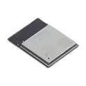
ESP32-S3-MINI-1-N8
ESP32-S3-MINI-1-N8 is a compact, low-power Wi-Fi and Bluetooth module from Espressif Systems based on the ESP32-S3 SoC. It integrates a dual-core Xtensa LX7 processor, 8 MB flash memory, crystal oscillator, RF matching circuitry, and a PCB antenna in a small SMD package, making it ideal for IoT devices, smart home products, industrial automation, HMI applications, AIoT edge devices, and USB-connected embedded systems. Key Features Dual-core 32-bit Xtensa LX7 CPU Up to 240 MHz operating frequency Includes single-precision floating-point unit (FPU) for enhanced processing performance. Integrated Memory 8 MB Quad SPI Flash (N8 variant) 512 KB SRAM 384 KB ROM 16 KB RTC SRAM. Wireless Connectivity 2.4 GHz Wi-Fi 4 (802.11 b/g/n) Data rates up to 150 Mbps Bluetooth 5 LE with Bluetooth Mesh support Simultaneous Wi-Fi and Bluetooth operation through an integrated coexistence mechanism. Rich Peripheral Set Up to 39 GPIOs USB 2.0 OTG USB Serial/JTAG SPI, I²C, I²S, UART PWM, MCPWM SDIO Host ADC Touch sensing Temperature sensor TWAI® (CAN 2.0 compatible) Timers and watchdogs. Integrated Components On-board 40 MHz crystal oscillator PCB antenna RF matching network Compact certified module design. Operating Conditions Supply voltage: 3.0 V to 3.6 V Operating temperature: −40°C to +85°C. Compliance RoHS and REACH compliant RF-certified module for simplified product development. #RF_transceiver #Module #Esp32
125 Uses
0 Stars
ESP32-C3-MINI-1-H4
ESP32-C3-MINI-1-H4 is a compact, low-power wireless module from Espressif Systems built around the ESP32-C3 SoC. It integrates a 32-bit RISC-V processor, 2.4 GHz Wi-Fi, Bluetooth 5 LE, onboard 4 MB flash memory, crystal oscillator, RF matching circuitry, and a PCB antenna in a small surface-mount package. The module is designed for IoT devices, smart home products, industrial automation, wearable electronics, and wireless sensor applications. Key Features 32-bit RISC-V single-core processor with clock speeds up to 160 MHz. 2.4 GHz Wi-Fi 4 (802.11 b/g/n) connectivity. Bluetooth 5 Low Energy (BLE 5.0) support with long-range capability. 4 MB embedded SPI flash memory (H4 variant). 384 KB ROM and 408 KB SRAM for application execution. Integrated PCB antenna for simplified RF design. USB Serial/JTAG controller for programming and debugging without an external USB-to-UART bridge. Multiple peripheral interfaces: UART SPI I²C I²S PWM GPIO ADC USB JTAG Operating voltage range: 3.0 V to 3.6 V. Supports secure boot, flash encryption, and hardware cryptographic acceleration. Compact SMD module suitable for space-constrained designs. Typical Applications Smart home and home automation devices Wireless sensors and data loggers IoT gateways and edge devices Industrial monitoring and control systems Bluetooth beacons Wearable electronics Consumer connected products H4 Variant Note: The ESP32-C3-MINI-1-H4 version includes 4 MB flash memory and supports an extended operating temperature range up to 105°C, making it suitable for more demanding industrial environments. #RF-Transceiver #ESP32 #Module
99 Uses
0 Stars
ESP32-C3-MINI-1-N4
The ESP32-C3-MINI-1-N4 is a compact, low-power wireless module from Espressif Systems built around the ESP32-C3 SoC. It integrates a 32-bit RISC-V single-core processor, 2.4 GHz Wi-Fi, Bluetooth 5 Low Energy (BLE), onboard flash memory, crystal oscillator, RF circuitry, and PCB antenna in a small surface-mount package. The module is designed for IoT devices, smart home products, industrial automation, sensor nodes, wearable devices, and other wireless embedded applications. Key Features 32-bit RISC-V Single-Core CPU Up to 160 MHz operating frequency Optimized for low-power IoT applications Integrated Memory 4 MB embedded Flash (N4 version) 400 KB SRAM 384 KB ROM 8 KB RTC SRAM Wireless Connectivity IEEE 802.11 b/g/n Wi-Fi (2.4 GHz) Data rates up to 150 Mbps Bluetooth 5 LE support Bluetooth Mesh capability Simultaneous Wi-Fi and Bluetooth operation using a shared antenna Security Features Secure Boot Flash Encryption Hardware cryptographic acceleration RSA, AES, HMAC, and Digital Signature support Rich Peripheral Set Up to 15 GPIOs UART SPI I²C I²S USB Serial/JTAG PWM TWAI (CAN 2.0 compatible) SAR ADC Timers and Watchdog timers Temperature sensor Integrated Components On-board PCB antenna 40 MHz crystal oscillator RF matching circuitry No external RF design required Power Supply Operating voltage: 3.0 V to 3.6 V Designed for low-power applications Environmental Specifications Operating temperature: −40°C to +85°C (N4 variant) RoHS and REACH compliant #module #RF-Transceiver #ESP32-C3
130 Uses
0 Stars
NRF52832-QFAA-R7
IC RF TxRx + MCU Bluetooth Bluetooth v5.3 2.4GHz 48-VFQFN Exposed Pad NRF52832-QFAA-R7 is an ultra-low-power wireless System-on-Chip (SoC) from Nordic Semiconductor, designed for Bluetooth Low Energy (BLE), ANT, NFC, and proprietary 2.4 GHz wireless applications. It integrates a high-performance ARM Cortex-M4F processor, memory, peripherals, and a 2.4 GHz radio into a single chip, making it ideal for IoT devices, wearables, wireless sensors, beacons, and smart peripherals. GHz protocols • 2.4 GHz transceiver • -96 dBm sensitivity in Bluetooth® low energy mode • Supported data rates: 1 Mbps, 2 Mbps Bluetooth® low energy mode • -20 to +4 dBm TX power, configurable in 4 dB steps • On-chip balun (single-ended RF) • 5.3 mA peak current in TX (0 dBm) • 5.4 mA peak current in RX • RSSI (1 dB resolution) • ARM® Cortex®-M4 32-bit processor with FPU, 64 MHz • 215 EEMBC CoreMark® score running from flash memory • 58 μA/MHz running from flash memory • 51.6 μA/MHz running from RAM • Data watchpoint and trace (DWT), embedded trace macrocell (ETM), and instrumentation trace macrocell (ITM) • Serial wire debug (SWD) • Trace port • Flexible power management • 1.7 V–3.6 V supply voltage range • Fully automatic LDO and DC/DC regulator system • Fast wake-up using 64 MHz internal oscillator • 0.3 μA at 3 V in System OFF mode • 0.7 μA at 3 V in System OFF mode with full 64 kB RAM retention • 1.9 μA at 3 V in System ON mode, no RAM retention, wake on RTC • Memory • 512 kB flash/64 kB RAM • 256 kB flash/32 kB RAM • Nordic SoftDevice ready • Support for concurrent multi-protocol • Type 2 near field communication (NFC-A) tag with wakeup-on-field and touchto-pair capabilities • 12-bit, 200 ksps ADC - 8 configurable channels with programmable gain • 64 level comparator • 15 level low power comparator with wakeup from System OFF mode • Temperature sensor • 32 general purpose I/O pins • 3x 4-channel pulse width modulator (PWM) unit with EasyDMA • Digital microphone interface (PDM) • 5x 32-bit timer with counter mode • Up to 3x SPI master/slave with EasyDMA • Up to 2x I2C compatible 2-wire master/slave • I2S with EasyDMA • UART (CTS/RTS) with EasyDMA • Programmable peripheral interconnect (PPI) • Quadrature decoder (QDEC) • AES HW encryption with EasyDMA • Autonomous peripheral operation without CPU intervention using PPI and EasyDMA • 3x real-time counter (RTC) • Single crystal operation • Package variants • QFN48 package, 6 × 6 mm • WLCSP package, 3.0 × 3.2 mm #CommonPartsLibrary #IntegratedCircuit
49 Uses
0 Stars
INA228AIDGSR
Power Supply Controller Digital Power Monitor 10-VSSOP The INA228 is an ultra-precise digital power monitor with a 20-bit delta-sigma ADC specifically designed for current-sensing applications. The device can measure a full-scale differential input of ±163.84 mV or ±40.96 mV across a resistive shunt sense element with common-mode voltage support from –0.3 V to +85 V. The INA228 reports current, bus voltage, temperature, power, energy and charge accumulation while employing a precision ±0.5% integrated oscillator, all while performing the needed calculations in the background. The integrated temperature sensor is ±1°C accurate for die temperature measurement and is useful in monitoring the system ambient temperature. The low offset and gain drift design of the INA228 allows the device to be used in precise systems that do not undergo multi-temperature calibration during manufacturing. Further, the very low offset voltage and noise allow for use in mA to kA sensing applications and provide a wide dynamic range without significant power dissipation losses on the sensing shunt element. The low input bias current of the device permits the use of larger currentsense resistors, thus providing accurate current measurements in the micro-amp range. The device allows for selectable ADC conversion times from 50 µs to 4.12 ms as well as sample averaging from 1x to 1024x, which further helps reduce the noise of the measured data. • High-resolution, 20-bit delta-sigma ADC • Current monitoring accuracy: – Offset voltage: ±1 µV (maximum) – Offset drift: ±0.01 µV/°C (maximum) – Gain error: ±0.05% (maximum) – Gain error drift: ±20 ppm/°C (maximum) – Common mode rejection: 154 dB (minimum) • Power monitoring accuracy: – 0.5% full scale, –40°C to +125°C (maximum) • Energy and charge accuracy: – 1.0% full scale (maximum) • Fast alert response: 75 μs • Wide common-mode range: –0.3 V to +85 V • Bus voltage sense input: 0 V to 85 V • Shunt full-scale differential range: ±163.84 mV / ±40.96 mV • Input bias current: 2.5 nA (maximum) • Temperature sensor: ±1°C (maximum at 25°C) • Programmable resistor temperature compensation • Programmable conversion time and averaging • 2.94-MHz high-speed I2C interface with 16 pinselectable addresses • Operates from a 2.7-V to 5.5-V supply: – Operational current: 640 µA (typical) – Shutdown current: 5 µA (maximum) #CommonPartsLibrary #IntegratedCircuit #PowerManagement
120 Uses
0 Stars