Microchip Technology
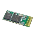
HC-05
HC-05 module is an easy to use Bluetooth SPP (Serial Port Protocol) module, designed for transparent wireless serial connection setup. Serial port Bluetooth module is fully qualified Bluetooth V2.0+EDR (Enhanced Data Rate) 3Mbps Modulation with complete 2.4GHz radio transceiver and baseband. It uses CSR Bluecore 04-External single chip Bluetooth system with CMOS technology and with AFH(Adaptive Frequency Hopping Feature). It has the footprint as small as 12.7mmx27mm. Hope it will simplify your overall design/development cycle #Module #Bluetooth #SPP
1.1k Uses
7 Stars
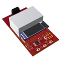
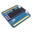
Arduino Watch Module
This module is a minimalist Arduino Watch design. Consisting of a Microchip ATTINY85-20SU microcontroller, an OLED display for visual output, two user buttons for interface, and a Li-ion Battery for power. The schematic also includes graphic user interface with ISP for programming and minimal passive components for functionality. #project #Template #projectTemplate #reusable #module #simple-embedded #microchip #arduino #sublayout
10 Uses
4 Stars
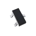
AO3400A
N-Channel 30 V 5.7A (Ta) 1.4W (Ta) Surface Mount SOT-23-3 The AO3400A N-Channel MOSFET is a 30V N-channel enhancement-mode MOSFET designed using trench MOSFET technology. It is widely used for load switching, DC-DC converters, motor driving, and PWM control applications due to its very low on-resistance and compact SOT-23 package. It is especially popular in small electronics and embedded systems because it can be driven directly by 3.3V or 5V logic signals, making it ideal for microcontroller-based designs. Key Features Drain-Source Voltage (VDS): 30V Continuous Drain Current (ID): up to 5.7A (at 25°C) Ultra-low RDS(on): ~26.5 mΩ @ VGS = 10V ~32 mΩ @ VGS = 4.5V ~48 mΩ @ VGS = 2.5V Logic-level gate drive (works well with MCU GPIOs) Fast switching performance (ns-range switching times) Low gate charge (~6–7 nC) → efficient switching Compact SOT-23 package for space-saving PCB design Low power dissipation (~1.4W typical at 25°C ambient) Operating temperature: −55°C to +150°C Typical Applications Load switching (LEDs, sensors, small motors) Power management in battery-powered devices DC-DC converters PWM control circuits Fan and heater control in embedded systems #AO3400A #MOSFET #NChannelMOSFET #PowerElectronics #SOT23 #LoadSwitch #EmbeddedSystems #ElectronicsComponents #TrenchMOSFET #Commonpartslibrary #Transistor #FET
2.5k Uses
3 Stars
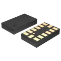
ADXL345BCCZ-RL
Accelerometer X, Y, Z Axis ±2g, 4g, 8g, 16g 0.05Hz ~ 1.6kHz 14-LGA (3x5) The ADXL345 is a small, thin, ultralow power, 3-axis accelerometer with high resolution (13-bit) measurement at up to ±16 g. Digital output data is formatted as 16-bit twos complement and is accessible through either a SPI (3- or 4-wire) or I2C digital interface. The ADXL345 is well suited for mobile device applications. It measures the static acceleration of gravity in tilt-sensing applications, as well as dynamic acceleration resulting from motion or shock. Its high resolution (3.9 mg/LSB) enables measurement of inclination changes less than 1.0°. Several special sensing functions are provided. Activity and inactivity sensing detect the presence or lack of motion by comparing the acceleration on any axis with user-set thresholds. Tap sensing detects single and double taps in any direction. Free-fall sensing detects if the device is falling. These functions can be mapped individually to either of two interrupt output pins. An integrated memory management system with a 32-level first in, first out (FIFO) buffer can be used to store data to minimize host processor activity and lower overall system power consumption. Low power modes enable intelligent motion-based power management with threshold sensing and active acceleration measurement at extremely low power dissipation. The ADXL345 is supplied in a small, thin, 3 mm × 5 mm × 1 mm, 14-lead, plastic package. ► Ultralow power: as low as 23 µA in measurement mode and 0.1 µA in standby mode at VS = 2.5 V (typical) ► Power consumption scales automatically with bandwidth ► User-selectable resolution ► Fixed 10-bit resolution ► Full resolution, where resolution increases with g range, up to 13-bit resolution at ±16 g (maintaining 4 mg/LSB scale factor in all g ranges) ► Embedded memory management system with FIFO technology minimizes host processor load ► Single tap/double tap detection ► Activity/inactivity monitoring ► Free-fall detection ► Supply voltage range: 2.0 V to 3.6 V ► I/O voltage range: 1.7 V to VS ► SPI (3- and 4-wire) and I2C digital interfaces ► Flexible interrupt modes mappable to either interrupt pin ► Measurement ranges selectable via serial command ► Bandwidth selectable via serial command ► Wide temperature range (−40°C to +85°C) ► 10,000 g shock survival ► Pb free/RoHS compliant #commonpartslibrary #sensor #transducer #accelerometer
199 Uses
2 Stars
ATMEGA328PB-AU
AVR series Microcontroller IC 8-Bit 20MHz 32KB (16K x 16) FLASH 32-TQFP (7x7) The ATMEGA328PB-AU is a low-power, high-performance 8-bit AVR microcontroller from Microchip Technology. It is an enhanced version of the widely used ATmega328P, offering additional peripherals while maintaining compatibility. It operates on the AVR RISC architecture, enabling efficient instruction execution with most instructions completed in a single clock cycle. This makes it suitable for embedded systems, industrial control, consumer electronics, and IoT applications. The device comes in a 32-pin TQFP package (AU) and integrates memory, analog features, communication interfaces, and timers into a compact solution. Key Features Core & Performance 8-bit AVR RISC CPU Up to 20 MHz clock frequency Single-cycle instruction execution for high efficiency Memory 32 KB Flash (with self-programming capability) 2 KB SRAM 1 KB EEPROM Peripherals & Interfaces 2 × USART (compared to 1 in ATmega328P) 2 × SPI interfaces 2 × I²C (TWI) interfaces Up to 23 programmable I/O pins Timers & PWM 3 Timers/Counters: 2 × 8-bit timers 1 × 16-bit timer Multiple PWM channels Analog Features 10-bit ADC (up to 8 channels) Analog comparator Power & Voltage Operating voltage: 1.8V to 5.5V Multiple low-power modes: Idle Power-down Power-save Standby Special Features Watchdog Timer with independent oscillator Brown-out Detection (BOD) In-System Programming (ISP) Debug support via debugWIRE Package & Temperature Package: TQFP-32 (AU) Operating temperature: Industrial grade: –40°C to +85°C#CommonPartsLibrary #Microcontroller #Atmega328
670 Uses
2 Stars
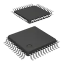
PIC16F877A-I/P
PIC PIC® 16F Microcontroller IC 8-Bit 20MHz 14KB (8K x 14) FLASH 40-PDIP The PIC16F877A-I/P is a high-performance 8-bit microcontroller from Microchip Technology, based on a Harvard architecture with separate program and data memory buses. It is designed for a wide range of embedded applications requiring reliable processing, multiple communication interfaces, and analog capability. The device integrates Flash program memory, EEPROM data storage, and numerous peripherals including ADC, timers, serial communication modules, and PWM functions. Packaged in a 40-pin PDIP form factor, it is widely used in industrial automation, consumer electronics, and educational development systems. Core Features 8-bit PIC microcontroller architecture Harvard architecture with RISC instruction set Operating frequency up to 20 MHz Single-cycle instruction execution (except branches) Memory Program Memory: 8K words (Flash) Data Memory (RAM): 368 bytes EEPROM Data Memory: 256 bytes I/O Features Up to 33 programmable I/O pins Multiple input/output ports (PORTA, PORTB, PORTC, PORTD, PORTE) High current sink/source capability on selected pins Analog Features 10-bit Analog-to-Digital Converter (ADC) Up to 8 analog input channels Programmable voltage reference Timers and Control Three timers (Timer0, Timer1, Timer2) Capture/Compare/PWM (CCP) modules Watchdog Timer (WDT) Power-on Reset (POR) and Brown-out Reset (BOR) Communication Interfaces USART (Universal Synchronous/Asynchronous Receiver/Transmitter) SPI (Serial Peripheral Interface) I²C (Inter-Integrated Circuit) via MSSP module Electrical Characteristics Operating Voltage: 4.0V to 5.5V Operating Temperature Range: -40°C to +85°C (Industrial grade) Low power consumption modes available Package Information Package Type: PDIP (Plastic Dual Inline Package) Pin Count: 40 pins Mounting Type: Through-hole Applications Industrial control systems Embedded automation Consumer electronics Sensor interfacing and data acquisition Educational and prototyping platforms #commonpartslibrary #integratedcircuit #microcontroller
867 Uses
2 Stars
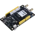
Wio-WM1110 Dev Kit
The Wio-WM1110 Dev Kit is an all-in-one solution for developing low-power, long-range IoT positioning applications. Based on Wio-WM1110 Wireless Module, features Semtech's LoRa® technology for long-range wireless communication, GNSS, and Wi-Fi for location tracking, and also supports Bluetooth Low Energy, Bluetooth mesh, NFC, Thread, and Zigbee.
3 Uses
2 Stars
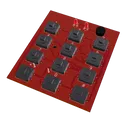
Keypad lock Module
This module involves the design of a keypad lock system. It utilizes an ATMEGA328P microcontroller, buzzers, LEDs for indicator functions and a 4x3 matrix keypad. An in-circuit serial programming (ISP) header is also present for programming the microcontroller. #template #lock #keypad #reusable #module #simple-embedded #microchip #arduino #atmega328 #TPS613222A #ISP #buzzer #sublayout
222 Uses
2 Stars
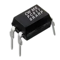
PC817C-S
SOP-4-2.54mm Transistor, Photovoltaic Output Optoisolators ROHS PC817C-S SOP-4_L6.5-W4.6-P2.54-LS10.3-TL LCSC Part Number: C3008369 JLCPCB Part Class: Extended Part Manufactured by UMW(友台半导体) The ESDA18-1K is a transient voltage suppression and electrostatic discharge protection device designed to protect sensitive electronic circuits from ESD events, surge transients, and electrical overstress conditions. Manufactured by STMicroelectronics and commonly used in communication and embedded electronic systems, this device provides fast-response protection for signal lines and low-voltage interfaces exposed to external electrical disturbances. The component utilizes low-capacitance TVS diode technology to clamp transient voltages while maintaining signal integrity on high-speed communication lines. It is optimized for protecting USB interfaces, GPIO lines, communication ports, sensor interfaces, and portable electronic devices from electrostatic discharge damage and transient spikes. The ESDA18-1K is widely used in industrial electronics, consumer devices, embedded systems, communication hardware, and portable equipment requiring compact and reliable ESD suppression. Its small surface-mount package enables easy integration into high-density PCB layouts while improving overall system reliability and EMC robustness. Engineering Specification Device Type Transient voltage suppression and ESD protection diode Protection Function Electrostatic discharge and surge transient suppression Protection Architecture Single-line TVS protection structure Response Characteristics Fast transient clamping response Signal Compatibility Suitable for low-voltage and high-speed signal interfaces Capacitance Characteristics Low capacitance for minimal signal distortion Electrical Performance Low leakage current and stable clamping behavior Reliability Features High ESD robustness and transient tolerance Mounting Style Surface mount technology Package Type Compact SOD-style surface-mount package Thermal Characteristics Low-power passive protection structure EMC Features Enhanced electromagnetic compatibility protection support Applications USB interface protection GPIO protection Communication interfaces Embedded systems Portable electronics Industrial control hardware Sensor interfaces Consumer electronics Signal line protection Data communication systems Manufacturer STMicroelectronics #commonpartslibrary #esdprotection #tvsdiode #transientprotection #signalprotection #stmicroelectronics #embeddedhardware #electronicsdesign
180 Uses
1 Star
HX711
Precision 24-bit analog-to-digital converter (ADC) designed for weigh scales and industrial control applications to interface directly with a bridge sensor. Based on Avia Semiconductor’s patented technology, HX711 is a precision 24-bit analogto-digital converter (ADC) designed for weigh scales and industrial control applications to interface directly with a bridge sensor. The input multiplexer selects either Channel A or B differential input to the low-noise programmable gain amplifier (PGA). Channel A can be programmed with a gain of 128 or 64, corresponding to a full-scale differential input voltage of ±20mV or ±40mV respectively, when a 5V supply is connected to AVDD analog power supply pin. Channel B has a fixed gain of 32. Onchip power supply regulator eliminates the need for an external supply regulator to provide analog power for the ADC and the sensor. Clock input is flexible. It can be from an external clock source, a crystal, or the on-chip oscillator that does not require any external component. On-chip poweron-reset circuitry simplifies digital interface initialization. There is no programming needed for the internal registers. All controls to the HX711 are through the pins. • Two selectable differential input channels • On-chip active low noise PGA with selectable gain of 32, 64 and 128 • On-chip power supply regulator for load-cell and ADC analog power supply • On-chip oscillator requiring no external component with optional external crystal • On-chip power-on-reset • Simple digital control and serial interface: pin-driven controls, no programming needed • Selectable 10SPS or 80SPS output data rate • Simultaneous 50 and 60Hz supply rejection • Current consumption including on-chip analog power supply regulator: normal operation < 1.5mA, power down < 1uA • Operation supply voltage range: 2.6 ~ 5.5V • Operation temperature range: -40 ~ +85℃ • 16 pin SOP-16 package #commonpartslibrary #integratedcircuit #analog #digital #converter #sensor
799 Uses
1 Star
STM32F405RGT6
ARM® Cortex®-M4 series Microcontroller IC 32-Bit Single-Core 168MHz 1MB (1M x 8) FLASH 64-LQFP (10x10) Arm® Cortex®-M4 32b MCU+FPU, 210DMIPS, up to 1MB flash/192+4KB RAM, USB OTG HS/FS, Ethernet, 17 TIMs, 3 ADCs, 15 comm. interfaces, and camera Includes ST state-of-the-art patented technology • Core: Arm® 32-bit Cortex®-M4 CPU with FPU, Adaptive real-time accelerator (ART Accelerator) allowing 0-wait state execution from flash memory, frequency up to 168 MHz, memory protection unit, 210 DMIPS/ 1.25 DMIPS/MHz (Dhrystone 2.1), and DSP instructions • Memories – Up to 1 Mbyte of flash memory – Up to 192+4 Kbytes of SRAM including 64- Kbyte of CCM (core coupled memory) data RAM – 512 bytes of OTP memory – Flexible static memory controller supporting CompactFlash™, SRAM, PSRAM, NOR and NAND memories • LCD parallel interface, 8080/6800 modes • Clock, reset, and supply management – 1.8 V to 3.6 V application supply and I/Os – POR, PDR, PVD and BOR – 4-to-26 MHz crystal oscillator – Internal 16 MHz factory-trimmed RC (1% accuracy) – 32 kHz oscillator for RTC with calibration – Internal 32 kHz RC with calibration • Low-power operation – Sleep, Stop, and Standby modes –VBAT supply for RTC, 20×32-bit backup registers + optional 4 KB backup SRAM • 3×12-bit, 2.4 MSPS A/D converters: up to 24 channels and 7.2 MSPS in triple interleaved mode • 2×12-bit D/A converters • General-purpose DMA: 16-stream DMA controller with FIFOs and burst support • Up to 17 timers: up to twelve 16-bit and two 32- bit timers up to 168 MHz, each with up to 4 IC/OC/PWM or pulse counter and quadrature (incremental) encoder input • Debug mode – Serial wire debug (SWD) & JTAG interfaces – Cortex-M4 Embedded Trace Macrocell™ • Up to 140 I/O ports with interrupt capability – Up to 136 fast I/Os up to 84 MHz – Up to 138 5 V-tolerant I/Os • Up to 15 communication interfaces – Up to 3 × I2C interfaces (SMBus/PMBus) – Up to 4 USARTs/2 UARTs (10.5 Mbit/s, ISO 7816 interface, LIN, IrDA, modem control) – Up to 3 SPIs (42 Mbits/s), 2 with muxed full-duplex I2S to achieve audio class accuracy via internal audio PLL or external clock – 2 × CAN interfaces (2.0B Active) – SDIO interface • Advanced connectivity – USB 2.0 full-speed device/host/OTG controller with on-chip PHY – USB 2.0 high-speed/full-speed device/host/OTG controller with dedicated DMA, on-chip full-speed PHY and ULPI – 10/100 Ethernet MAC with dedicated DMA: supports IEEE 1588v2 hardware, MII/RMII #commonpartslibrary #integratedcircuit #microcontroller
53 Uses
1 Star

PS21964-4S
The Mitsubishi PS21964-4S is a dual-in-line package intelligent power module that integrates a transfer-mold type insulated design suitable for 600V/15A applications. This component combines low-loss 5th generation IGBT inverter bridge technology dedicated to three-phase DC-to-AC power conversion with open emitter configuration. It is designed with embedded drive circuits, high voltage high-speed level shifting, under-voltage protection for both upper and lower leg IGBTs, short circuit protection for lower-leg IGBTs, and system control functionalities into a compact package. The module supports fault signaling corresponding to short circuit faults in the lower-leg IGBT or under-voltage conditions, offering an integrated solution for AC100V~200V inverter drive applications in small power motor controls. With its UL approval (Yellow Card No. E80276) and featuring an input interface compatible with 3V and 5V lines (High Active), the PS21964-4S is engineered to cater to a broad range of industrial applications demanding reliable and efficient power conversion and control.
28 Uses
1 Star
Wio-WM1110 Wireless Module
The Wio-WM1110 is a fusion positioning module for developing low-power, long-range IoT applications. It's embedded with Semtech LR1110 and Nordic nRF52840, features Semtech's LoRa technology for long-range wireless communication, GNSS, Wi-Fi, and Bluetooth for location tracking services.
45 Uses
1 Star
Wio-WM1110 Dev Kit
The Wio-WM1110 Dev Kit is an all-in-one solution for developing low-power, long-range IoT positioning applications. Based on Wio-WM1110 Wireless Module, features Semtech's LoRa® technology for long-range wireless communication, GNSS, and Wi-Fi for location tracking, and also supports Bluetooth Low Energy, Bluetooth mesh, NFC, Thread, and Zigbee.
0 Uses
1 Star
Seeed studio Wio-WM1110 Wireless
The Wio-WM1110 is a fusion positioning module for developing low-power, long-range IoT applications. It's embedded with Semtech LR1110 and Nordic nRF52840, features Semtech's LoRa technology for long-range wireless communication, GNSS, Wi-Fi, and Bluetooth for location tracking services.
4 Uses
1 Star
Energy Meter Module
This is an Energy Meter project leveraging an ATTiny85 microcontroller (U1) to sense current through an ACS712 module (U2). It displays the data in real-time on an OLED display (OLED1) and interacts with three buttons (NEXT, MENU, OK). This compact energy meter is suitable for edge computing and low-power Internet of Things (IoT) applications #project #keypad #arduino #attiny85 #ISP #reusable #module #edge-computing #edgeComputing #microchip #sublayout
29 Uses
1 Star
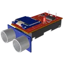
Ultrasonic Distance Meter Module
This circuit is an ultrasonic distance meter based on an ATTiny2313 microcontroller. It uses an HC-SR04 ultrasonic sensor to measure distance and displays the results on an OLED display. The power supply is constructed using a Boost converter (TPS613222A) and a 2-cell AA battery. Additionally, it also includes ISP for programming, RESET and START switches, and LED indicators. #project #Template #projectTemplate #ultrasonic #OLED #arduino #attiny2313 #TPS613222A #ISP #reusable #module #simple-embedded #microchip #sublayout
112 Uses
1 Star