Analog Devices
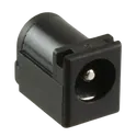
PJ-202A
Power Barrel Connector Jack 2.10mm ID (0.083"), 5.50mm OD (0.217") Through Hole, Right Angle The PJ-202A is a DC power jack connector (barrel jack) commonly used in electronic devices to provide a stable DC power input. It is designed for through-hole PCB mounting and supports a right-angle (horizontal) orientation, making it suitable for compact PCB layouts. This connector typically mates with a 2.0 mm center-pin DC plug and is widely used in consumer electronics, routers, embedded systems, and small power supply boards. Key Features Connector Type: DC power jack (barrel type) Center Pin Size: 2.0 mm Outer Diameter Compatibility: ~6.5 mm plug type Mounting Style: Through-hole Orientation: Right-angle / horizontal PCB mount Rated Current: up to 2.5 A Rated Voltage: up to 24 V DC ontact Configuration: 2 conductors with internal switch option Durability: ~5,000 insertion cycles Operating Temperature: -25°C to +85°C Flammability Rating: UL94V-0 plastic housing Typical Applications Embedded systems Arduino / DIY electronics power input Consumer electronics Router / modem power input Battery-powered device charging inputs DC-005 barrel jack #commonpartslibrary #connector #barrel #jack #tht
116 Uses
3 Stars
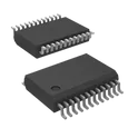
TB6612FNG,C,8,EL
Motor Driver Power MOSFET Parallel 24-SSOP The TB6612FNG,C,8,EL is a dual H-bridge motor driver IC developed by Toshiba. It is designed to control the speed and direction of two DC motors or one bipolar stepper motor. This device uses low ON-resistance MOSFETs for efficient operation, resulting in lower heat generation and higher efficiency compared to traditional bipolar transistor-based drivers. It is widely used in robotics, motor control applications, and embedded systems. Key Features Motor Drive Capability Dual H-bridge driver (can drive 2 DC motors or 1 stepper motor) Output current: 1.2 A (continuous) per channel 3.2 A (peak) per channel Wide motor supply voltage range: 2.5 V to 13.5 V Logic & Control Logic supply voltage (VCC): 2.7 V to 5.5 V Compatible with 3.3 V and 5 V microcontrollers (e.g., ESP32, Arduino) Control inputs: IN1, IN2 (per channel for direction control) PWM input for speed control STBY (standby mode for power saving) Efficiency & Performance Low ON-resistance MOSFETs: Reduces power loss and heat High efficiency compared to L298N-type drivers Built-in shoot-through protection Protection Features Thermal shutdown protection Overcurrent protection Under voltage lockout (UVLO) #Commonpartslibrary #Motordriver #Integratedcircuit #TB6612
76.8k Uses
3 Stars
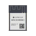
ESP32-C6-WROOM-1-N4
802.15.4 Bluetooth, Wi-Fi Bluetooth v5.0, ZigBee® Transceiver Module 2.4GHz PCB Trace Surface Mount The ESP32-C6-WROOM-1-N4 is based on the ESP32-C6 single-core RISC-V microcontroller, integrating advanced wireless standards and secure connectivity in a small module format. It is designed for next-generation IoT devices that require Wi-Fi 6 efficiency, mesh networking, and Bluetooth Low Energy support. Processor: 32-bit RISC-V single-core CPU (up to 160 MHz) Wireless Connectivity: Wi-Fi 6 (802.11ax, 2.4 GHz) Bluetooth LE 5.0 IEEE 802.15.4 (Thread / Zigbee support) Memory (N4 variant): 4 MB Flash Security: Secure boot Flash encryption Cryptographic hardware acceleration #commonpartslibrary #rf #wireless #transceiver #module #zigbee
363 Uses
3 Stars
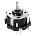
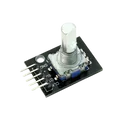
KY-040
KY-040 rotary encoder is a device that generates an electrical signal based upon how much the rotary input device (knob) is rotated and the direction it is rotating in. It is a position sensor with a knob and can be used to control stepper or servo motors with precision. #Module #Rotary-Encoder
614 Uses
3 Stars
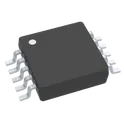
MAX98357AETE+T
MAX98357A Series 5.5V 3.2W PCM Input Class D Audio Power Amplifier - TQFN-16 The MAX98357A/MAX98357B is an easy-to-use, low-cost, digital pulse-code modulation (PCM) input Class D amplifier that provides industry-leading Class AB audio performance with Class D efficiency. The digital audio interface automatically recognizes up to 35 different PCM and TDM clocking schemes which eliminates the need for I2C programming. Operation is further simplified by eliminating the need for an external MCLK signal that is typically used for PCM communication. Simply supply power, LRCLK, BCLK, and digital audio to generate audio! Furthermore, a novel pinout allows customers to use the cost-effective WLP package with no need for expensive vias (refer to Application Note 6643: Optimize Cost, Size, and Performance with MAX98357 WLP for more information). The digital audio interface is highly flexible with the MAX98357A supporting I2S data and the MAX98357B supporting left-justified data. Both ICs support 8 channel time division multiplexed (TDM) data. The digital audio interface accepts specified sample rates between 8kHz and 96kHz for all supported data formats. The ICs can be configured to produce a left channel, right channel, or (left/2 + right/2) output from the stereo input data. The ICs operate using 16/24/32-bit data for I2S and left-justified modes as well as 16-bit or 32-bit data using TDM mode. The ICs eliminate the need for the external MCLK signal that is typically used for PCM communication. This reduces EMI and possible board coupling issues in addition to reducing the size and pin count of the ICs. The ICs also feature a very high wideband jitter tolerance (12ns typ) on BCLK and LRCLK to provide robust operation. Active emissions-limiting, edge-rate limiting, and overshoot control circuitry greatly reduce EMI. A filterless spread-spectrum modulation scheme eliminates the need for output filtering found in traditional Class D devices and reduces the component count of the solution. The ICs are available in 9-pin WLP (1.345mm x 1.435mm x 0.64mm) and 16-pin TQFN (3mm x 3mm x 0.75mm) packages and are specified over the -40°C to +85°C temperature range. ● Single-Supply Operation (2.5V to 5.5V) ● 3.2W Output Power into 4Ω at 5V ● 2.4mA Quiescent Current ● 92% Efficiency (RL = 8Ω, POUT = 1W) ● 22.8μVRMS Output Noise (AV = 15dB) ● Low 0.013% THD+N at 1kHz ● No MCLK Required ● Sample Rates of 8kHz to 96kHz ● Supports Left, Right, or (Left/2 + Right/2) Output ● Sophisticated Edge Rate Control Enables Filterless Class D Outputs ● 77dB PSRR at 1kHz ● Low RF Susceptibility Rejects TDMA Noise from GSM Radios ● Extensive Click-and-Pop Reduction Circuitry ● Robust Short-Circuit and Thermal Protection ● Available in Space-Saving Packages: 1.345mm x 1.435mm WLP (0.4mm Pitch) and 3mm x 3mm TQFN ● Solution Size with Single Bypass Capacitor is 4.32mm2 Applications ● Single Li-ion Cell/5V Devices ● Smart Speakers ● Notebook Computers ● IoT Devices ● Gaming Devices (Audio and Haptics) ● Smartphones ● Tablets ● Cameras #commonpartslibrary #integratedcircuit #linearamplifier #mono
975 Uses
2 Stars
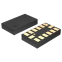
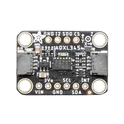
ADXL345BCCZ-RL
Accelerometer X, Y, Z Axis ±2g, 4g, 8g, 16g 0.05Hz ~ 1.6kHz 14-LGA (3x5) The ADXL345 is a small, thin, ultralow power, 3-axis accelerometer with high resolution (13-bit) measurement at up to ±16 g. Digital output data is formatted as 16-bit twos complement and is accessible through either a SPI (3- or 4-wire) or I2C digital interface. The ADXL345 is well suited for mobile device applications. It measures the static acceleration of gravity in tilt-sensing applications, as well as dynamic acceleration resulting from motion or shock. Its high resolution (3.9 mg/LSB) enables measurement of inclination changes less than 1.0°. Several special sensing functions are provided. Activity and inactivity sensing detect the presence or lack of motion by comparing the acceleration on any axis with user-set thresholds. Tap sensing detects single and double taps in any direction. Free-fall sensing detects if the device is falling. These functions can be mapped individually to either of two interrupt output pins. An integrated memory management system with a 32-level first in, first out (FIFO) buffer can be used to store data to minimize host processor activity and lower overall system power consumption. Low power modes enable intelligent motion-based power management with threshold sensing and active acceleration measurement at extremely low power dissipation. The ADXL345 is supplied in a small, thin, 3 mm × 5 mm × 1 mm, 14-lead, plastic package. ► Ultralow power: as low as 23 µA in measurement mode and 0.1 µA in standby mode at VS = 2.5 V (typical) ► Power consumption scales automatically with bandwidth ► User-selectable resolution ► Fixed 10-bit resolution ► Full resolution, where resolution increases with g range, up to 13-bit resolution at ±16 g (maintaining 4 mg/LSB scale factor in all g ranges) ► Embedded memory management system with FIFO technology minimizes host processor load ► Single tap/double tap detection ► Activity/inactivity monitoring ► Free-fall detection ► Supply voltage range: 2.0 V to 3.6 V ► I/O voltage range: 1.7 V to VS ► SPI (3- and 4-wire) and I2C digital interfaces ► Flexible interrupt modes mappable to either interrupt pin ► Measurement ranges selectable via serial command ► Bandwidth selectable via serial command ► Wide temperature range (−40°C to +85°C) ► 10,000 g shock survival ► Pb free/RoHS compliant #commonpartslibrary #sensor #transducer #accelerometer
198 Uses
2 Stars
ADXL345
ADXL345 iMEMS® Accelerometer, 3 Axis Sensor Evaluation Board The ADXL345 measures acceleration in three axes (X, Y, Z) and outputs digital data via either I²C or SPI interfaces. It is widely used in applications like tilt sensing, vibration monitoring, free-fall detection, and motion-based user interfaces. Its high resolution (up to 13-bit) allows it to detect very small changes in motion, making it suitable for both consumer electronics and industrial applications. Key Features 3-axis acceleration measurement (X, Y, Z) Selectable measurement ranges: ±2g, ±4g, ±8g, ±16g High resolution (13-bit) with up to 4 mg/LSB sensitivity Digital output interfaces: I²C and SPI Low power consumption: ideal for battery-powered devices Built-in motion detection functions: Tap and double-tap detection Free-fall detection Activity and inactivity monitoring Wide bandwidth range: supports various data rates for different applications Operating voltage: typically 2.0V to 3.6V Compact package: small LGA form factor suitable for space-constrained designs Common Applications Smartphones and tablets (screen rotation, motion sensing) Wearable devices and fitness trackers Gaming controllers Robotics and drones Vibration and shock monitoring systems #commonpartslibrary #developmentboard #evaluationboard #sensor
120 Uses
2 Stars
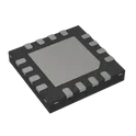
ATMEGA328PB-AU
AVR series Microcontroller IC 8-Bit 20MHz 32KB (16K x 16) FLASH 32-TQFP (7x7) The ATMEGA328PB-AU is a low-power, high-performance 8-bit AVR microcontroller from Microchip Technology. It is an enhanced version of the widely used ATmega328P, offering additional peripherals while maintaining compatibility. It operates on the AVR RISC architecture, enabling efficient instruction execution with most instructions completed in a single clock cycle. This makes it suitable for embedded systems, industrial control, consumer electronics, and IoT applications. The device comes in a 32-pin TQFP package (AU) and integrates memory, analog features, communication interfaces, and timers into a compact solution. Key Features Core & Performance 8-bit AVR RISC CPU Up to 20 MHz clock frequency Single-cycle instruction execution for high efficiency Memory 32 KB Flash (with self-programming capability) 2 KB SRAM 1 KB EEPROM Peripherals & Interfaces 2 × USART (compared to 1 in ATmega328P) 2 × SPI interfaces 2 × I²C (TWI) interfaces Up to 23 programmable I/O pins Timers & PWM 3 Timers/Counters: 2 × 8-bit timers 1 × 16-bit timer Multiple PWM channels Analog Features 10-bit ADC (up to 8 channels) Analog comparator Power & Voltage Operating voltage: 1.8V to 5.5V Multiple low-power modes: Idle Power-down Power-save Standby Special Features Watchdog Timer with independent oscillator Brown-out Detection (BOD) In-System Programming (ISP) Debug support via debugWIRE Package & Temperature Package: TQFP-32 (AU) Operating temperature: Industrial grade: –40°C to +85°C#CommonPartsLibrary #Microcontroller #Atmega328
667 Uses
2 Stars