Microcontrollers
A microcontroller is a small, low-cost computer-on-a-chip that can be used to control electronic devices and systems. It consists of a central processing unit (CPU), memory, input/output (I/O) ports, and other peripherals integrated onto a single chip. Microcontrollers are commonly used in a wide range of applications, including automotive systems, home appliances, industrial automation, and consumer electronics. One of the key benefits of microcontrollers is their ability to interact with their environment through sensors and actuators, making them well-suited for use in embedded systems. These systems are often found in devices that require real-time control or data processing, such as medical equipment, aircraft, and factory automation systems. Flux.ai is home to the world's largest community-driven public library of microcontrollers, with footprints, symbols, datasheets, and simulation models for a wide range of devices. Whether you're a professional engineer looking for a specific microcontroller for your next project, or a hobbyist exploring the possibilities of microcontroller-based systems, Flux.ai has the resources you need to get started.
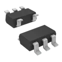
AP2112K-3.3TRG1
Linear Voltage Regulator IC Positive Fixed 1 Output 600mA SOT-25 3.3V LDO AP2112K-3.3 The AP2112K-3.3TRG1 is a low dropout (LDO) linear voltage regulator designed to provide a stable 3.3V output from a higher input voltage. It is optimized for low noise, high power supply rejection ratio (PSRR), and low quiescent current, making it suitable for battery-powered and noise-sensitive applications. The device features current limiting and thermal shutdown protection, ensuring reliable operation under fault conditions. It is commonly used in portable electronics, RF modules, microcontroller power supplies, and other low-power systems. Key Features Fixed output voltage: 3.3V Output current: up to 600 mA Low dropout voltage: ~250 mV at 300 mA load High PSRR: up to 70 dB at 1 kHz Low quiescent current: typically 55 µA Stable with low ESR ceramic capacitors Built-in overcurrent protection Thermal shutdown protection Fast transient response Absolute Maximum Ratings Input Voltage (VIN): up to 6.5 V Output Current: Internally limited Operating Junction Temperature: -40°C to +125°C Storage Temperature: -65°C to +150°C Electrical Characteristics (Typical values unless otherwise specified) Output Voltage Accuracy: ±2% Dropout Voltage: 250 mV @ 300 mA 400 mV @ 600 mA Line Regulation: 0.05%/V Load Regulation: 0.2% Quiescent Current: 55 µA Shutdown Current: <1 µA PSRR: 70 dB @ 1 kHz 45 dB @ 10 kHz Pin Configuration (SOT-23-5 / SC-70-5) VIN – Input voltage GND – Ground EN – Enable (active high) NC – No connection VOUT – Regulated output (3.3V) Package Information Package Type: SOT-23-5 (TRG1 suffix indicates tape & reel) Mounting: Surface mount Small footprint suitable for compact PCB layouts Typical Applications Battery-powered devices Wireless modules (Wi-Fi, Bluetooth, RF) Microcontroller and FPGA power supplies Portable consumer electronics Sensor and analog circuits requiring low noise Compliance & Reliability RoHS compliant Lead-free package Designed for high reliability and long operational life #CommonPartsLibrary #IntegratedCircuit #PowerManagement #LinearRegulator #VoltageRegulator
3.2k Uses1 StarsESP32-P4NRW32
QFN-104(10x10) Microcontrollers RoHS Wireless microcontroller module for embedded processing and wireless communication, designed to provide integrated compute and RF connectivity for IoT applications. #ESPRESSIF #MCUModule #WirelessModule #IoT #CommonPartsLibrary #IntegratedCircuit #microcontroller
153 Uses1 Stars