Microcontrollers
A microcontroller is a small, low-cost computer-on-a-chip that can be used to control electronic devices and systems. It consists of a central processing unit (CPU), memory, input/output (I/O) ports, and other peripherals integrated onto a single chip. Microcontrollers are commonly used in a wide range of applications, including automotive systems, home appliances, industrial automation, and consumer electronics. One of the key benefits of microcontrollers is their ability to interact with their environment through sensors and actuators, making them well-suited for use in embedded systems. These systems are often found in devices that require real-time control or data processing, such as medical equipment, aircraft, and factory automation systems. Flux.ai is home to the world's largest community-driven public library of microcontrollers, with footprints, symbols, datasheets, and simulation models for a wide range of devices. Whether you're a professional engineer looking for a specific microcontroller for your next project, or a hobbyist exploring the possibilities of microcontroller-based systems, Flux.ai has the resources you need to get started.
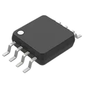
MCP9808T-E/MS
Temperature Sensor Digital, Local -40°C ~ 125°C 10 b 8-MSOP The MCP9808T-E/MS is a high-accuracy digital temperature sensor developed by Microchip Technology for precision thermal monitoring applications. The device communicates through a standard I²C-compatible serial interface and is optimized for low-power embedded systems requiring accurate ambient temperature measurement. It integrates internal temperature sensing, analog-to-digital conversion, programmable alert functionality, and configurable power management within a compact MSOP package. The sensor is designed for applications including industrial monitoring, consumer electronics, IoT devices, thermal management systems, medical instrumentation, and battery-powered portable equipment. Its low operating current and shutdown capability make it suitable for energy-efficient systems where thermal accuracy and minimal power consumption are critical. The device supports programmable temperature limits and interrupt generation for over-temperature events, enabling autonomous thermal supervision without continuous host processor intervention. The MCP9808T-E/MS maintains high measurement accuracy across a wide operating temperature range and offers stable digital output without requiring external calibration components. Electrical Characteristics Supply voltage operation supports low-voltage and standard logic systems. Low operating current enables efficient continuous monitoring. Shutdown mode significantly reduces power consumption during inactive periods. Digital I²C interface supports standard and fast communication modes. Integrated temperature conversion engine provides direct digital temperature output. Temperature Sensing Features High-accuracy ambient temperature measurement. Wide operating temperature range suitable for industrial environments. Programmable resolution for balancing conversion speed and precision. Configurable upper, lower, and critical temperature alert thresholds. Integrated hysteresis control for stable thermal event detection. Communication Interface I²C-compatible serial communication interface. Configurable slave addressing for multi-device bus operation. Supports read and write access to internal configuration registers. Compatible with common microcontrollers and embedded processors. Functional Features Integrated alert output for thermal event signaling. Programmable interrupt and comparator operating modes. Internal registers support temperature monitoring and device configuration. Power-on reset circuitry ensures predictable startup behavior. Device identification registers support system-level verification. Mechanical Characteristics Package type is MSOP with compact surface-mount footprint. Suitable for automated PCB assembly processes. RoHS-compliant and lead-free manufacturing. Typical Applications Industrial temperature monitoring systems. Portable battery-powered electronics. Embedded microcontroller systems. Thermal protection and supervision circuits. Consumer and IoT sensing devices. Medical and laboratory instrumentation. #CommonPartsLibrary #Sensor #Transducer #Temperature-Sensor #MCP9808
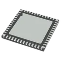
22 Uses0 StarsDSPIC33CK128MP205-I/M4
dsPIC dsPIC™ 33CK, Functional Safety (FuSa) Microcontroller IC 16-Bit 100MHz 128KB (128K x 8) FLASH 48-UQFN (6x6) 28/36/48/64/80-Pin Digital Signal Controllers with High-Resolution PWM and CAN Flexible Data (CAN FD) perating Conditions • 3.0V to 3.6V, -40°C to +125°C, DC to 100 MIPS • 3.0V to 3.6V, -40°C to +150°C, DC to 70 MIPS Core: 16-Bit dsPIC33CK CPU • 32-256 Kbytes of Program Flash with ECC and 8-24K RAM • Fast 6-Cycle Divide • LiveUpdate • Code Efficient (C and Assembly) Architecture • 40-Bit Wide Accumulators • Single-Cycle (MAC/MPY) with Dual Data Fetch • Single-Cycle, Mixed-Sign MUL Plus Hardware Divide • 32-Bit Multiply Support • Four Sets of Interrupt Context Saving Registers which Include Accumulator and STATUS for Fast Interrupt Handling • Zero Overhead Looping • RAM Memory Built-In Self-Test (MBIST) Clock Management • Internal Oscillator • Programmable PLLs and Oscillator Clock Sources • Reference Clock Output • Fail-Safe Clock Monitor (FSCM) • Fast Wake-up and Start-up • Backup Internal Oscillator Power Management • Low-Power Management Modes (Sleep, Idle, Doze) • Integrated Power-on Reset and Brown-out Reset High-Speed PWM • Eight PWM Pairs • Up to 250 ps PWM Resolution • Dead Time for Rising and Falling Edges • Dead-Time Compensation • Clock Chopping for High-Frequency Operation • PWM Support for: - DC/DC, AC/DC, inverters, PFC, lighting - BLDC, PMSM, ACIM, SRM motors • Fault and Current Limit Inputs • Flexible Trigger Configuration for ADC Triggering Timers/Output Compare/Input Capture • One General Purpose Timer • Peripheral Trigger Generator (PTG): - Up to 15 trigger sources to other peripheral modules - CPU independent state machine-based instruction sequencer • Nine MCCP/SCCP modules which Include Timer, Capture/Compare and PWM: - One MCCP - Eight SCCPs - 16 or 32-bit time base - 16 or 32-bit capture - 4-deep capture buffer • Fully Asynchronous Operation, Available in Sleep Modes
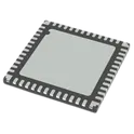
3 Uses0 StarsdsPIC33CK256MP205-I/M4
dsPIC dsPIC™ 33CK, Functional Safety (FuSa) Microcontroller IC 16-Bit 100MHz 256KB (256K x 8) FLASH 48-UQFN (6x6) 28/36/48/64/80-Pin Digital Signal Controllers with High-Resolution PWM and CAN Flexible Data (CAN FD) Operating Conditions • 3.0V to 3.6V, -40°C to +125°C, DC to 100 MIPS • 3.0V to 3.6V, -40°C to +150°C, DC to 70 MIPS Core: 16-Bit dsPIC33CK CPU • 32-256 Kbytes of Program Flash with ECC and 8-24K RAM • Fast 6-Cycle Divide • LiveUpdate • Code Efficient (C and Assembly) Architecture • 40-Bit Wide Accumulators • Single-Cycle (MAC/MPY) with Dual Data Fetch • Single-Cycle, Mixed-Sign MUL Plus Hardware Divide • 32-Bit Multiply Support • Four Sets of Interrupt Context Saving Registers which Include Accumulator and STATUS for Fast Interrupt Handling • Zero Overhead Looping • RAM Memory Built-In Self-Test (MBIST) Clock Management • Internal Oscillator • Programmable PLLs and Oscillator Clock Sources • Reference Clock Output • Fail-Safe Clock Monitor (FSCM) • Fast Wake-up and Start-up • Backup Internal Oscillator Power Management • Low-Power Management Modes (Sleep, Idle, Doze) • Integrated Power-on Reset and Brown-out Reset High-Speed PWM • Eight PWM Pairs • Up to 250 ps PWM Resolution • Dead Time for Rising and Falling Edges • Dead-Time Compensation • Clock Chopping for High-Frequency Operation • PWM Support for: - DC/DC, AC/DC, inverters, PFC, lighting - BLDC, PMSM, ACIM, SRM motors • Fault and Current Limit Inputs • Flexible Trigger Configuration for ADC Triggering Timers/Output Compare/Input Capture • One General Purpose Timer • Peripheral Trigger Generator (PTG): - Up to 15 trigger sources to other peripheral modules - CPU independent state machine-based instruction sequencer • Nine MCCP/SCCP modules which Include Timer, Capture/Compare and PWM: - One MCCP - Eight SCCPs - 16 or 32-bit time base - 16 or 32-bit capture - 4-deep capture buffer • Fully Asynchronous Operation, Available in Sleep Modes #CommonPartsLibrary #IntegratedCircuit #Microcontroller #DSPIC33CK256MP
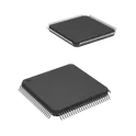
11 Uses0 StarsSTM32F407VGT6
ARM Microcontrollers - MCU ARM M4 1024 FLASH 168 Mhz 192kB SRAM 100-LQFP (14x14) Arm® Cortex®-M4 32b MCU+FPU, 210DMIPS, up to 1MB Flash/192+4KB RAM, USB OTG HS/FS, Ethernet, 17 TIMs, 3 ADCs, 15 comm. interfaces & camera • Core: Arm® 32-bit Cortex®-M4 CPU with FPU, Adaptive real-time accelerator (ART Accelerator) allowing 0-wait state execution from Flash memory, frequency up to 168 MHz, memory protection unit, 210 DMIPS/ 1.25 DMIPS/MHz (Dhrystone 2.1), and DSP instructions • Memories – Up to 1 Mbyte of Flash memory – Up to 192+4 Kbytes of SRAM including 64- Kbyte of CCM (core coupled memory) data RAM – 512 bytes of OTP memory – Flexible static memory controller supporting Compact Flash, SRAM, PSRAM, NOR and NAND memories • LCD parallel interface, 8080/6800 modes • Clock, reset and supply management – 1.8 V to 3.6 V application supply and I/Os – POR, PDR, PVD and BOR – 4-to-26 MHz crystal oscillator – Internal 16 MHz factory-trimmed RC (1% accuracy) – 32 kHz oscillator for RTC with calibration – Internal 32 kHz RC with calibration • Low-power operation – Sleep, Stop and Standby modes –VBAT supply for RTC, 20×32 bit backup registers + optional 4 KB backup SRAM • 3×12-bit, 2.4 MSPS A/D converters: up to 24 channels and 7.2 MSPS in triple interleaved mode • 2×12-bit D/A converters • General-purpose DMA: 16-stream DMA controller with FIFOs and burst support • Up to 17 timers: up to twelve 16-bit and two 32- bit timers up to 168 MHz, each with up to 4 IC/OC/PWM or pulse counter and quadrature (incremental) encoder input • Debug mode – Serial wire debug (SWD) & JTAG interfaces – Cortex-M4 Embedded Trace Macrocell™ • Up to 140 I/O ports with interrupt capability – Up to 136 fast I/Os up to 84 MHz – Up to 138 5 V-tolerant I/Os • Up to 15 communication interfaces – Up to 3 × I2C interfaces (SMBus/PMBus) – Up to 4 USARTs/2 UARTs (10.5 Mbit/s, ISO 7816 interface, LIN, IrDA, modem control) – Up to 3 SPIs (42 Mbits/s), 2 with muxed full-duplex I2S to achieve audio class accuracy via internal audio PLL or external clock – 2 × CAN interfaces (2.0B Active) – SDIO interface • Advanced connectivity – USB 2.0 full-speed device/host/OTG controller with on-chip PHY – USB 2.0 high-speed/full-speed device/host/OTG controller with dedicated DMA, on-chip full-speed PHY and ULPI – 10/100 Ethernet MAC with dedicated DMA: supports IEEE 1588v2 hardware, MII/RMII #CommonPartsLibrary #IntegratedCircuit #Microcontroller #STM32F407
43 Uses0 StarsMIMXRT1176DVMAA
ARM® Cortex®-M4, Cortex®-M7 RT1170 Microcontroller IC 32-Bit Dual-Core 400MHz, 800MHz External Program Memory 289-LFBGA (14x14) Pre-ordered MCUs MIMXRT1176DVMAA MAPBGA-289_L14.0-W14.0-R17-C17-P0.80-TL LCSC Part Number: C1020237 JLCPCB Part Class: Extended Part Manufactured by NXP(恩智浦)
50 Uses0 StarsSN65HVD230DR
1/1 Transceiver Half CANbus 8-SOIC The SN65HVD230DR is a high-speed Controller Area Network (CAN) transceiver designed to interface a CAN protocol controller with the physical two-wire CAN bus. It operates as a differential line driver and receiver, translating logic-level signals into robust bus-level signals suitable for automotive, industrial, and distributed control applications. The device is optimized for reliable communication in electrically noisy environments and supports low-power operation, making it suitable for systems requiring energy efficiency and extended operational stability. This transceiver conforms to widely adopted CAN physical layer standards and is intended for use in systems requiring high data integrity, fault tolerance, and electromagnetic compatibility. It integrates protection features and supports standby functionality to reduce system power consumption when communication is inactive. Functional Overview The device provides bidirectional signal conversion between a CAN controller and the differential CAN bus lines. It features a transmit data input and a receive data output, enabling full-duplex communication at the protocol level. The driver stage generates differential output signals on the bus, while the receiver stage detects and translates bus signals back into logic-level data. An internal control mechanism allows the device to enter a low-power standby mode, reducing current consumption when active communication is not required. The transceiver includes slope control capability to manage signal edge rates, which helps minimize electromagnetic interference and improves signal integrity across the network. Electrical Characteristics The transceiver operates from a single low-voltage supply and is designed for compatibility with modern microcontrollers and digital logic systems. It provides differential output drive capability with controlled rise and fall characteristics. The receiver is designed with high input sensitivity and noise immunity to ensure accurate signal detection under varying bus conditions. The device includes thermal protection and safeguards against bus faults, including short-circuit conditions. Its internal circuitry is designed to maintain stable operation across a wide range of environmental conditions and supply variations. Interface Requirements The logic interface is compatible with standard digital input and output levels, allowing direct connection to a CAN controller. The bus interface consists of two differential lines that connect to the CAN network. Proper termination and layout practices are required to ensure optimal communication performance and compliance with CAN network design guidelines. Operating Conditions The device is intended for operation across a broad temperature range suitable for industrial and automotive environments. It maintains functional integrity under typical voltage fluctuations and environmental stresses encountered in embedded systems. Protection and Reliability Features The transceiver incorporates protection mechanisms to guard against overcurrent, thermal overload, and electrostatic discharge. It is designed to maintain communication reliability even in the presence of transient disturbances and electrical noise. Packaging and Integration The SN65HVD230DR is provided in a compact surface-mount package suitable for automated assembly. Its pin configuration supports straightforward integration into printed circuit board designs with minimal external components. #CommonPartsLibrary #IntegratedCircuits #Interface #Drivers #Receivers #Transceivers #65HVD230
98 Uses0 StarsTPD1E05U06DPYR
14V Clamp 2.5A (8/20µs) Ipp Tvs Diode Surface Mount 2-X1SON (1x.60) TVS diode USB VBUS 5V TVS diode USB VBUS 5V ESD protection General Description The TPD1E05U06DPYR is a single-channel transient voltage suppression device designed to protect sensitive electronic components from electrostatic discharge (ESD) and other transient voltage events. It is engineered for high-speed signal applications, offering low capacitance to preserve signal integrity while providing robust protection. The device is suitable for integration into compact and portable electronic systems where space, reliability, and performance are critical. Device Identification Part number: TPD1E05U06DPYR Device classification: ESD protection diode / transient voltage suppressor Manufacturer: Commonly associated with Texas Instruments Mounting type: Surface-mount Package style: Ultra-small leadless package (e.g., X2SON/DFN) Functional Description Protects circuits from high-voltage transients caused by ESD events Limits voltage spikes by clamping them to safe levels Maintains signal quality by minimizing added capacitance Operates transparently under normal signal conditions Provides fast response to transient disturbances Performance Characteristics Low capacitance suitable for high-speed data lines High ESD protection capability compliant with standard test models Low leakage current during normal operation Fast transient response time Stable performance across specified operating conditions Electrical Characteristics Designed for low-voltage applications (approximately 5 V working range) Low clamping voltage to protect downstream components Minimal dynamic resistance Very low input/output capacitance High reliability under repeated ESD stress Application Scope High-speed communication interfaces such as USB, HDMI, and display ports Mobile phones, tablets, and wearable electronics Embedded systems and microcontroller interfaces Consumer and industrial electronic equipment Data and signal line protection in compact devices Mechanical and Physical Properties Compact footprint for high-density PCB layouts Leadless package for improved mechanical robustness Compatible with standard surface-mount assembly processes Designed for automated manufacturing environments Integration Guidelines Install as close as possible to the external connector or entry point Ensure a low-impedance path to ground for optimal protection Minimize trace length between the device and the protected line Consider layout practices to preserve high-speed signal integrity Verify compatibility with system voltage and interface requirements #commonpartslibrary #circuitprotection #tvsdiode
664 Uses0 Stars