Memory
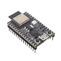
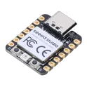
Seeed Studio XIAO RP2040
The Seeed Studio XIAO RP2040 is as small as the Seeed Studio XIAO SAMD21 but it's more powerful. On one hand, it carries the powerful Dual-core RP2040 processor that can flexible clock running up to 133 MHz which is a low-power microcontrollers. On the Seeed Studio XIAO RP2040 there is also 264KB of SRAM, and 2MB of on-board Flash memory which can provide more program to save and run. On the other hand, this little board has good performance in processing but needs less power. All in all, it is designed in a tiny size as small as a thumb(20x17.5mm) and can be used for wearable devices and small projects.
12 Uses
1 Star

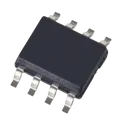
AT24C04D-XHM
SOP65P640X120-8N http://ww1.microchip.com/downloads/en/devicedoc/atmel-8896e-seeprom-at24c04d-datasheet.pdf Atmel AT24C04D-XHM-B EEPROM Memory Chip, 4kbit, 1.7 3.6 V 8-Pin TSSOP 1.2 Microchip AT24C04D-XHM-B 556-AT24C04D-XHM-B https://www.mouser.co.uk/ProductDetail/Microchip-Technology-Atmel/AT24C04D-XHM-B?qs=E2PpAYvlWVuNqXOGsLWx2Q%3D%3D AT24C04D-XHM-B https://www.arrow.com/en/products/at24c04d-xhm-b/microchip-technology
9 Uses
1 Star
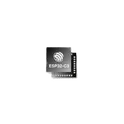
ESP32-C3
Bluetooth, WiFi 802.11b/g/n, Bluetooth v5.0 Transceiver Module 2.402GHz ~ 2.48GHz Antenna Not Included Surface Mount The ESP32-C3 is a low-power, highly integrated 32-bit microcontroller (MCU) from Espressif Systems that combines 2.4 GHz Wi-Fi and Bluetooth® 5 Low Energy (BLE) connectivity in a single chip. Built around a single-core RISC-V processor running at up to 160 MHz, it is designed for secure, cost-effective IoT and embedded applications. The ESP32-C3 offers excellent wireless performance, low power consumption, robust security features, and a rich set of peripherals, making it ideal for smart home devices, industrial automation, wearable electronics, wireless sensors, and consumer IoT products. Key Features 32-bit RISC-V single-core CPU running up to 160 MHz Integrated 2.4 GHz Wi-Fi (802.11 b/g/n) and Bluetooth® 5 LE Low-power architecture with multiple sleep modes for battery-powered devices Advanced security features including Secure Boot, Flash Encryption, AES, SHA, RSA, HMAC, and hardware random number generator (RNG) Rich peripheral set including GPIO, UART, SPI, I²C, I²S, PWM, ADC, TWAI (CAN), USB Serial/JTAG, and timers Supports external QSPI flash memory and OTA (Over-the-Air) firmware updates Compact package options suitable for space-constrained embedded designs Fully supported by the ESP-IDF, Arduino, and MicroPython development ecosystems #ESP32C3 #Espressif #RISCV #WiFi #BluetoothLE #IoT #EmbeddedSystems #Microcontroller #WirelessMCU #LowPower #SmartHome #IndustrialIoT #SecureMCU #EdgeComputing #FirmwareDevelopment
9 Uses
0 Stars
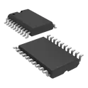
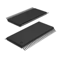
SN74CBT16390DL
Multiplexer/Demultiplexer 16 x 1:2 56-SSOP The SN74CBT16390 is a 16-bit to 32-bit switch used in applications in which two separate data paths must be multiplexed onto, or demultiplexed from, a single path. This device can be used for memory interleaving, in which two different banks of memory must be addressed simultaneously. This device also can be used to connect or isolate the PCI bus to one or two slots simultaneously. Two output enables (OE1 and OE2) control the data flow. When OE1 is low, A port is connected to 1B port. When OE2 is low, A port is connected to 2B port. When both OE1 and OE2 are low, the A port is connected to both 1B and 2B ports. The control inputs can be driven with a 5-V CMOS, 5-V TTL, or an LVTTL driver. Key Features 16-bit to 32-bit FET multiplexer/demultiplexer bus switch Operates from 4.5 V to 5.5 V Low ON-state resistance for high-speed signal switching Near-zero propagation delay through the switch Dual output-enable (OE1, OE2) controls for flexible routing TTL-compatible control inputs Supports memory interleaving and PCI bus applications Low power consumption ESD protection compliant with JESD22 standards Operating temperature range: −40°C to +85°C Available in a 56-pin SSOP (DL) package #BusSwitch #Multiplexer #Demultiplexer #Widebus #DigitalLogic #HighSpeedInterface #MemoryInterleaving #PCIBus #TexasInstruments #SN74CBT16390 #SSOP56
0 Uses
0 Stars
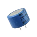
FT0H474ZF
470 mF (EDLC) Supercapacitor 5.5 V Radial, Can 6.5Ohm @ 1kHz The FT0H474ZF is a 5.5 V electric double-layer capacitor (EDLC), also known as a supercapacitor, manufactured by KEMET. It provides 470 mF (0.47 F) of capacitance for energy storage, backup power, and short-duration power hold-up applications. Designed for through-hole mounting in a radial can package, it offers high reliability, a wide operating temperature range, and long cycle life, making it suitable for memory backup, RTC backup, industrial electronics, and low-power energy storage systems. Key Features 470 mF (0.47 F) capacitance 5.5 V rated voltage Electric Double-Layer Capacitor (EDLC) technology Radial through-hole package Long operational life with excellent charge/discharge cycle capability Wide operating temperature range: −40°C to +85°C Low maintenance energy storage solution Suitable for backup power, memory retention, and peak power assistance RoHS compliant Reliable performance for industrial and consumer electronic applications #KEMET #Supercapacitor #EDLC #EnergyStorage #BackupPower #MemoryBackup #PowerHoldUp #RadialCapacitor #ThroughHole #Electronics #IndustrialElectronics #LowPowerDesign #CommonPartsLibrary #Capacitor
0 Uses
0 Stars
MSPM0C1104S8YCJR
ARM® Cortex®-M0+ MSPM0 C Microcontroller IC 32-Bit 24MHz 16KB (16K x 8) FLASH 8-DSBGA (0.86x1.6) MSPM0C110x microcontrollers (MCUs) are part of the MSP highly-integrated ultra-low-power 32-bit MCU family based on the enhanced Arm® Cortex®-M0+ core platform operating at up to 24MHz frequency. These costoptimized MCUs offer high-performance analog peripheral integration, support extended temperature ranges from -40°C to 125°C, and operate with supply voltages from 1.62V to 3.6V. The MSPM0C110x devices provide up to 16KB embedded flash program memory with 1KB SRAM. These MCUs incorporate a high-speed on-chip oscillator with an accuracy from -2% to +1.2%, eliminating the need for an external crystal. Additional features include a 1-channel DMA, CRC-16 accelerator, and a variety of highperformance analog peripherals such as one 12-bit 1.5Msps ADC with VDD as the voltage reference, and an on-chip temperature sensor. These devices also offer intelligent digital peripherals such as one 16-bit advanced timer, two 16-bit general purpose timer, one windowed watchdog timer, and a variety of communication peripherals including one UART, one SPI, and one I2C. These communication peripherals offer protocol support for LIN, IrDA, DALI, Manchester, smart card, SMBus, and PMBus. The TI MSPM0 family of low-power MCUs consists of devices with varying degrees of analog and digital integration let customers find the MCU that meets their project needs. The architecture combined with extensive low-power modes is optimized to achieve extended battery life in portable measurement applications. MSPM0C110x MCUs are supported by an extensive hardware and software ecosystem with reference designs and code examples to get the design started quickly. Development kits include a LaunchPad™ kit available for purchase and design files for a target-socket board. TI also provides a free MSP Software Development Kit (SDK), which is available as a component of Code Composer Studio™ IDE desktop and cloud version within the TI Resource Explorer. MSPM0 MCUs are also supported by extensive online collateral, training with MSP Academy, and online support through the TI E2E™ support forums. Features • Core – Arm® 32-bit Cortex®-M0+ CPU, frequency up to 24MHz • Operating characteristics – Extended temperature: –40°C to 125°C – Wide supply voltage range: 1.62V to 3.6V • Memories – Up to 16KB of flash – 1KB of SRAM • High-performance analog peripherals – One analog-to-digital converter (ADC) with up to 10 total external channels, 1.7Msps at 10 bit or 1.5Msps at 12 bit with VDD as the voltage reference – Configurable 1.4V or 2.5V internal ADC voltage reference (VREF) – Integrated temperature sensor – Integrated supply monitor • Optimized low-power modes – RUN: 87µA/MHz – STOP: 609µA at 4MHz, 311µA at 32kHz – STANDBY: 5µA with SRAM retention – SHUTDOWN: 200nA • Intelligent digital peripherals – 1-channel DMA controller dedicated for ADC – Three timers supporting up to 14 PWM channels • One 16-bit advanced timers with deadband support up to 8 PWM channels • One 16-bit general purpose timer with 4 capture/compares • One 16-bit general purpose timer with 2 capture/compares – Windowed watchdog timer – BEEPER generating 1kHz, 2kHz, 4kHz, or 8kHz square wave to drive the external beeper • Enhanced communication interfaces – One UART interface supporting LIN, IrDA, DALI, smart card, Manchester and low-power operation in STANDBY mode – One I2C interface supporting FM+ (1Mbps), SMBus, PMBus, and wakeup from STOP mode – One SPI supporting up to 12Mbps • Clock system – Internal 24MHz oscillator with an accuracy from -2% to +1.2% (SYSOSC) – Internal 32kHz low-frequency oscillator (LFOSC) • Data integrity – Cyclic redundancy checker (CRC-16) • Flexible I/O features – Up to 18 GPIOs – Two 5V-tolerant open-drain IOs • Development support – 2-pin serial wire debug (SWD) • Package options – 20-pin TSSOP (PW) – 20-pin VSSOP (DGS) – 20-pin WQFN (RUK) – 16-pin SOT (DYY) – 8-pin SOT (DDF) – 8-pin WSON (DSG) – 8-pin DSBGA (YCJ) • Family members (also see Device Comparison) – MSPS003F4: 16KB of flash, 1KB of RAM – MSPS003F3: 8KB of flash, 1KB of RAM – MSPM0C1104: 16KB of flash, 1KB of RAM – MSPM0C1103: 8KB of flash, 1KB of RAM • Development kits and software (also see Tools and Software) – LP-MSPM0C1104 LaunchPad™ development kit – MSP Software Development Kit (SDK) 2 Applications • Battery charging and management • Power supplies and power delivery • Personal electronics • Building security and fire safety • Connected peripherals and printers • Grid infrastructure • Smart metering • Communication modules • Medical and healthcare • Lighting #MSPM0C1104S8YCJR #MSPM0C1104 #TexasInstruments #CortexM0Plus #Microcontroller #EmbeddedSystems #LowPowerMCU #IoT #WearableDevices #IndustrialControl #ConsumerElectronics #ADC #UART #SPI #I2C #PWM #TI #ElectronicsDesign #PCBDesign #EmbeddedDevelopment
1 Use
0 Stars
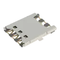
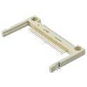
1734451-1
50 Position Card Connector CompactFlash® - Type I, II Surface Mount, Right Angle Gold 1734451-1 is a 50-position CompactFlash (CF) card connector from TE Connectivity. It is a low-profile, right-angle, surface-mount connector designed for interfacing CompactFlash Type I and Type II memory cards with a printed circuit board (PCB). The connector features gold-plated contacts for reliable signal transmission and durability, making it suitable for embedded systems, industrial equipment, data acquisition devices, and legacy storage applications. This part is currently marked as obsolete by the manufacturer. Key Features 50-position CompactFlash card connector Supports CompactFlash Type I and Type II cards Right-angle PCB mounting orientation Surface-mount termination (SMT) 1.27 mm contact pitch Gold-plated contact mating area Brass contacts with nickel underplating Low-profile connector design Maximum contact current rating: 0.5 A per contact Thermoplastic housing, UL 94V-0 rated Designed for signal transmission applications Board-mount connector with hold-down feature Obsolete product status #TEConnectivity #CompactFlash #CFCardConnector #MemoryConnector #PCCardSocket #EmbeddedSystems #SMTConnector #RightAngleConnector #PCBDesign #ElectronicComponents #IndustrialElectronics #DataStorage #ConnectorSolution #HardwareDesign #ObsoletePart
0 Uses
0 Stars
SIWG917Y111MGABAR
Bluetooth, WiFi 802.11b/g/n/ax, Bluetooth v5.4 Transceiver Module 2.4GHz Integrated, Chip Surface Mount Silicon Labs SiWG917 module is our lowest power Wi-Fi 6 plus Bluetooth LE 5.4, ideal for ultra-low power IoT wireless devices using Wi-Fi®, Bluetooth, Matter, and IP networking for secure cloud connectivity. It is optimal for developing battery operated devices that need long battery life. SiWG917 module includes an ultra-low power Wi-Fi 6 plus Bluetooth Low Energy (LE) 5.4 wireless CPU subsystem, and an integrated micro-controller (MCU) application subsystem, security, peripherals and power management subsystem all in a single 16 x 21.1 x 2.3 mm package. The wireless subsystem consists of a multi-threaded Network Wireless Processor (NWP) running up to 160 MHz, baseband digital signal processing, analog front end, 2.4 GHz RF transceiver and integrated power amplifier. The application subsystem consists of an ARM® Cortex®-M4 running up to 180 MHz, embedded SRAM, flash, ultra-low power sensor hub, and matrix vector processor. The ARM® Cortex®-M4 is dedicated for peripheral and application-related processing, while the NWP runs the wireless and networking stacks on independent threads, thus providing a fully integrated solution that is ready for a wide range of embedded wireless IoT applications. The modules come with modular radio type approvals for various countries, including USA (FCC), Canada (IC/ISED) and Japan (MIC), and are in compliance with the relevant EN standards (including EN 300 328 v2.2.2) for the conformity with the directives and regulations in EU and UK. KEY FEATURES • Wi-Fi 6 Single Band 2.4 GHz 20 MHz 1x1 stream IEEE 802.11 b/g/n/ax • Bluetooth LE 5.4 • Single chip Matter Over Wi-Fi Solution • ARM® Cortex® M4 Processor with FPU subsystem up to 180 MHz with rich set of Digital and Analog Peripherals. • Wi-Fi 6 Benefits: TWT for improved efficiency and longer battery life, MUMIMO/OFDMA for Higher Throughput, network capacity and low latency • Best in Class Device and Wireless Security • WLAN Tx power up to +17.5 dBm with integrated PA • Bluetooth LE Tx power up to +17 dBm with integrated PA • WLAN Rx sensitivity as low as -95.5 dBm • Wi-Fi 4 Standby Associated mode current: 71 μA @ 1-second listen interval • Embedded Flash option up to 8 MB/ optional external Flash up to 16 MB • Embedded PSRAM option up to 2 MB/ optional external PSRAM option up to 16 MB • Ultra-low power sensor hub peripherals • Matrix Vector Processor (MVP) • Embedded Wi-Fi, Bluetooth LE, Matter, and networking stacks supporting wireless coexistence • Three software-configurable MCU application memory options for sharing the RAM between the wireless, system, and application (192/256/320 KB) • Operating temperature: -40 to +85 ºC • Operating supply range: 3.0 to 3.63 V • Supply voltage for GPIOs: 1.71 to 3.63 V #WiFi6 #BluetoothLE54 #IoTModule #WirelessSoC #SiliconLabs #EmbeddedSystems #SmartHome #IndustrialIoT #LowPowerDesign #RFModule #ConnectedDevices #EdgeComputing #MatterReady #PCBDesign #ElectronicsEngineering
6 Uses
0 Stars
STM32H533RET6
ARM® Cortex®-M33 STM32H5 Microcontroller IC 32-Bit 250MHz 512KB (512K x 8) FLASH 64-LQFP (10x10) The STM32H533RET6 specification defines the engineering requirements for a high-performance embedded microcontroller designed for advanced control, computation, and communication applications. This specification establishes the functional, electrical, mechanical, environmental, and quality requirements necessary to ensure reliable operation in complex embedded systems across industrial, consumer, and communication environments. The device is intended for use in applications requiring real-time processing capability, efficient peripheral integration, and secure system operation. It supports embedded control systems, industrial automation, sensor data processing, communication gateways, and other applications requiring deterministic performance and flexible connectivity. Engineering Requirements The microcontroller shall be manufactured using advanced semiconductor processes to ensure high processing efficiency, low power consumption, and long-term operational reliability. The device shall support stable execution of embedded firmware under defined electrical, thermal, and environmental conditions. The architecture shall provide integrated memory resources, high-speed processing capability, and a wide range of peripheral interfaces to support system-level integration. Communication interfaces and on-chip peripherals shall operate reliably under specified conditions without degradation of performance or data integrity. Electrical characteristics shall ensure stable logic operation, accurate timing behavior, and robust signal integrity during normal operation, reset events, and power transitions. The device shall maintain functional stability under dynamic load conditions and environmental variation. Mechanical and package construction shall be suitable for surface-mount assembly and shall ensure mechanical robustness during soldering, handling, and operation. Workmanship shall be free from defects such as contamination, cracks, deformation, or structural inconsistencies that could impact performance or reliability. Inspection, validation, and testing shall be performed using controlled procedures and calibrated equipment to ensure compliance with all applicable engineering and quality requirements. Any deviation from this specification shall require formal engineering review, documented justification, and approval through established change control processes. Documentation Supporting documentation shall include official datasheets, reference manuals, qualification reports, electrical characterization data, inspection records, and revision-controlled manufacturing documentation. All records shall be maintained under formal configuration management and quality assurance systems. Revision Control Any modification to this specification shall be managed through the formal engineering change control system. All revisions shall undergo technical evaluation, validation, and approval prior to implementation to ensure continued compliance with design intent and applicable standards. #EngineeringSpecification #Microcontroller #STM32H5 #STMicroelectronics #EmbeddedSystems #RealTimeControl #IndustrialElectronics #Firmware #Semiconductor #QualityAssurance #EngineeringDocumentation
0 Uses
0 Stars
STM32F427IIT6
ARM® Cortex®-M4 STM32F4 Microcontroller IC 32-Bit 180MHz 2MB (2M x 8) FLASH 176-LQFP (24x24) The STM32F427IIT6 specification defines the engineering requirements for a high-performance microcontroller device designed for embedded processing applications requiring advanced computational capability, rich peripheral integration, and reliable real-time control. This specification establishes the functional, electrical, mechanical, environmental, and quality requirements necessary to ensure consistent operation across industrial, consumer, and communication systems. The device is intended for use in complex embedded systems where high-speed processing, efficient memory handling, and extensive peripheral connectivity are required. It supports applications such as industrial automation, motor control, signal processing, communication interfaces, and advanced embedded control systems. Engineering Requirements The microcontroller shall be manufactured using advanced semiconductor fabrication processes to ensure high processing performance, low power consumption, and long-term reliability. The device shall provide stable operation across its intended voltage, temperature, and environmental conditions while maintaining deterministic real-time behavior. The integrated architecture shall support high-speed processing capabilities, embedded memory resources, and multiple communication interfaces for system-level integration. Peripheral functionality shall operate reliably under defined electrical and environmental conditions without degradation of performance. Electrical characteristics shall ensure stable logic levels, accurate timing behavior, and robust signal integrity across all supported operating modes. The device shall maintain functional reliability during power transitions, reset conditions, and dynamic load variations. Mechanical and package construction shall be suitable for surface-mount assembly processes and shall ensure mechanical integrity during soldering, handling, and operation. Workmanship shall be free from defects including contamination, physical damage, or structural inconsistencies that could impact reliability or performance. Inspection, validation, and testing shall be performed using controlled procedures and calibrated equipment to ensure compliance with all applicable engineering and quality standards. Any deviation from this specification shall require formal engineering review, documented justification, and approval through the established change control process. Documentation Supporting documentation shall include engineering datasheets, reference manuals, qualification reports, electrical characterization data, inspection records, and revision-controlled manufacturing documentation. All records shall be maintained under formal configuration management and quality assurance systems. Revision Control Any modification to this specification shall be processed through the established engineering change management system. All revisions shall undergo technical review, validation, and formal approval prior to implementation to ensure continued compliance with design intent and applicable industry requirements. #EngineeringSpecification #Microcontroller #EmbeddedSystems #STMicroelectronics #DigitalControl #IndustrialElectronics #Firmware #Semiconductor #QualityAssurance #EngineeringDocumentation #RealTimeSystems
0 Uses
0 Stars
STM32G491RET6
ARM® Cortex®-M4F STM32G4 Microcontroller IC 32-Bit 170MHz 512KB (512K x 8) FLASH 64-LQFP (10x10) The STM32G491RET6 from STMicroelectronics is a high-performance 32-bit microcontroller based on the Arm® Cortex®-M4 core with Floating Point Unit (FPU), designed for advanced embedded applications requiring high computational performance, precise analog processing, and real-time control. It belongs to the STM32G4 series and integrates enhanced analog peripherals, motor-control timers, communication interfaces, security features, and hardware accelerators such as CORDIC and FMAC. The device operates at up to 170 MHz, provides 512 KB Flash memory, and includes 96 KB SRAM, making it suitable for applications such as motor control, digital power conversion, industrial automation, robotics, and embedded control systems. Key Features Core: Arm® Cortex®-M4 32-bit CPU with FPU, DSP instructions, and MPU Maximum CPU Frequency: Up to 170 MHz (up to 213 DMIPS) Memory: 512 KB Flash memory with ECC support 96 KB SRAM with parity checking features Quad-SPI memory interface Operating Voltage: 1.71 V to 3.6 V Package: LQFP-64 Advanced Analog Features: 3 × 12-bit ADCs with high-speed conversion 4 × 12-bit DAC channels 4 × Rail-to-Rail operational amplifiers 4 × Fast analog comparators Internal voltage reference buffer Hardware Accelerators: CORDIC accelerator for trigonometric calculations FMAC (Filter Math Accelerator) for digital filtering applications Timers & Motor Control: Advanced PWM timers for motor-control applications Multiple 16-bit and 32-bit timers Support for encoder and PWM control Communication Interfaces: 2 × FDCAN interfaces 5 × USART/UART 3 × SPI interfaces 3 × I²C interfaces USB 2.0 Full-Speed interface SAI audio interface Security Features: True Random Number Generator (TRNG) CRC calculation unit Unique device ID Debug & Programming: SWD and JTAG debugging support Typical Applications Motor control and BLDC controllers Digital power converters Industrial automation equipment Robotics and motion control Smart sensors and embedded control systems Power management applications #STM32G491RET6 #STM32G4 #STMicroelectronics #ARM_CortexM4 #Microcontroller #MCU #EmbeddedSystems #MotorControl #DigitalPower #IndustrialAutomation #Robotics #IoT #ElectronicsDesign #PCBDesign
6 Uses
0 Stars
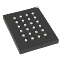
IS66WVH64M8DBLL-166B1LI
PSRAM (Pseudo SRAM) Memory IC 512Mbit HyperBus 166 MHz 36 ns 24-TFBGA (6x8) The IS66/67WVH64M8DALL/BLL are 512Mb Dual Die device containing two units of 256Mbit Pseudo Static Random Access Memory, organized as 64M words by 8 bits. The device supports a HyperBus interface, Very Low Signal Count (Address, Command and data through 8 DQ pins), Hidden Refresh Operation, and Automotive Temperature Operation, designed especially for Mobile and Automotive applications Key Features 512-Mbit (64M × 8) HyperRAM™ PSRAM High-speed HyperBus interface Clock frequency up to 166 MHz Fast 36 ns access time Single-ended clock architecture with reduced pin count Operating voltage range: 2.7 V to 3.6 V Industrial temperature range: −40°C to +85°C Low-power volatile memory solution Surface-mount 24-TFBGA (6 mm × 8 mm) package Suitable for graphics, AI edge devices, networking, and embedded systems requiring large external memory capacity. #CommonPartsLibrary #IntegratedCircuit #HyperRAM #PSRAM #ISSI #MemoryIC #HyperBus #EmbeddedSystems #IndustrialElectronics #IoT #HighSpeedMemory #BGA #VolatileMemory #EdgeComputing #HMI #ElectronicsDesign
1 Use
0 Stars
SN74HCT245DWR
SN74HCT245 / SN54HCT245 – octal bus transceiver with 3-state outputs designed for bidirectional data communication between two 8-bit buses. Features direction control (DIR) for selecting data flow direction and output enable (OE) for bus isolation. TTL-compatible inputs, low power consumption, and high-current outputs make it suitable for interfacing microcontrollers, memory devices, processors, FPGAs, LCD modules, industrial controllers, and digital communication systems. Operates from a 4.5 V to 5.5 V supply voltage and supports asynchronous data transfer. Search Keywords: SN74HCT245, SN54HCT245, HCT245, Octal Bus Transceiver, Bidirectional Bus Transceiver, 8 Bit Bus Buffer, 3 State Buffer, Tri State Buffer, TTL Compatible Logic IC, Data Bus Interface, Logic Level Buffer, Microcontroller Interface, Memory Bus Driver, Digital Logic IC, Bus Isolation IC, Direction Controlled Buffer, Parallel Data Interface, Industrial Control Logic, FPGA Interface, Processor Bus Transceiver Hashtags: #SN74HCT245 #SN54HCT245 #HCT245 #BusTransceiver #OctalBusTransceiver #TriStateBuffer #LogicIC #TTLCompatible #DigitalLogic #BusBuffer #MicrocontrollerInterface #FPGA #EmbeddedSystems #MemoryInterface #IndustrialElectronics #DataBus #ElectronicsDesign #PCBDesign #HardwareDesign #TexasInstruments
22 Uses
0 Stars
74HC238N
3-to-8 line decoder/demultiplexer The 74HC238; 74HCT238 decodes three binary weighted address inputs (A0, A1 and A2) to eight mutually exclusive outputs (Y0 to Y7). The device features three enable inputs (E1 and E2 and E3). Every output will be LOW unless E1 and E2 are LOW and E3 is HIGH. This multiple enable function allows easy parallel expansion to a 1-of-32 (5 to 32 lines) decoder with just four '238 ICs and one inverter. The '238 can be used as an eight output demultiplexer by using one of the active LOW enable inputs as the data input and the remaining enable inputs as strobes. Inputs include clamp diodes. This enables the use of current limiting resistors to interface inputs to voltages in excess of VCC. • Wide supply voltage range from 2.0 to 6.0 V • CMOS low power dissipation • High noise immunity • Demultiplexing capability • Multiple input enable for easy expansion • Ideal for memory chip select decoding • Active HIGH mutually exclusive outputs • Input levels: • For 74HC238: CMOS level • For 74HCT238: TTL level • Complies with JEDEC standards • JESD8C (2.7 V to 3.6 V) • JESD7A (2.0 V to 6.0 V) • Latch-up performance exceeds 100 mA per JESD 78 Class II Level B • ESD protection: • HBM: ANSI/ESDA/JEDEC JS-001 class 2 exceeds 2000 V • CDM: ANSI/ESDA/JEDEC JS-002 class C3 exceeds 1000 V • Multiple package options • Specified from -40 °C to +85 °C and from -40 °C to +125 °C #74HC238N #74HCSeries #CMOSLogic #DecoderIC #Demultiplexer #DigitalLogic #AddressDecoder #ChipSelect #LogicGate #IntegratedCircuit #ElectronicsDesign #EmbeddedSystems
0 Uses
0 Stars
ESP32-C3-DEVKITM-1
ESP32-C3-MINI-1 ESP32-C 802.11 b/g/n (WiFi/WLAN/Wi-Fi 4), Bluetooth® 5.x (BLE) Transceiver 2.4GHz Evaluation Board ESP32-C3-DevKitM-1 is a compact entry-level development board from Espressif Systems based on the ESP32-C3-MINI-1 module. It integrates a 32-bit RISC-V single-core microcontroller, 2.4 GHz Wi-Fi, and Bluetooth Low Energy (BLE) connectivity, making it suitable for IoT devices, embedded applications, smart sensors, and wireless control projects. The board exposes most GPIO pins through headers for easy prototyping and supports programming through USB. Key Features: 32-bit RISC-V Single-Core Processor Based on ESP32-C3 SoC architecture Clock frequency up to 160 MHz Wireless Connectivity Integrated 2.4 GHz Wi-Fi (802.11 b/g/n) Bluetooth 5 Low Energy (BLE) support Memory 4 MB embedded Flash memory inside the ESP32-C3-MINI-1 module GPIO and Peripheral Interfaces Multiple programmable GPIO pins Supports interfaces such as: SPI UART I²C I²S PWM ADC USB Serial/JTAG Development Board Features Built-in ESP32-C3-MINI-1 module with PCB antenna USB interface for programming and power 5 V to 3.3 V onboard voltage regulator Breadboard-friendly pin headers Applications IoT gateways Smart home devices Wireless sensors Industrial automation Wearable electronics Embedded control systems #ESP32C3 #ESP32 #DevKitM1 #Espressif #RISCVD #WiFiMCU #BluetoothLE #IoT #EmbeddedSystems #Microcontroller #WirelessModule #SmartDevices #ElectronicsDesign #Prototyping
7 Uses
0 Stars
MX66UM1G45GXDI00
Macronix MX66UM1G45G – 1 Gbit (128 MB) Octal SPI (xSPI) Serial NOR Flash memory designed for high-performance embedded systems. Supports Octal I/O interface for high-speed code execution, firmware storage, data logging, graphics assets, and external memory expansion. Features sector, block, and chip erase operations, page programming, status monitoring, low-power standby mode, and endurance of up to 100,000 program/erase cycles. Suitable for microcontrollers, processors, industrial systems, automotive electronics, networking equipment, IoT devices, HMI displays, and embedded Linux applications. Search Keywords: MX66UM1G45G, Macronix Flash Memory, Octal SPI Flash, OctaFlash, xSPI Flash, Serial NOR Flash, 1Gbit Flash Memory, 128MB Flash, External Flash Memory, Boot Flash, Firmware Storage, Execute In Place Flash, XIP Memory, High Speed Flash Memory, Embedded Storage, Industrial Flash Memory, Automotive Flash Memory, MCU External Memory, Processor Boot Memory, Non Volatile Memory MX66UM1G45G Hashtags: #MX66UM1G45G #Macronix #OctalSPI #OctaFlash #xSPI #NORFlash #SerialFlash #FlashMemory #ExternalMemory #NonVolatileMemory #FirmwareStorage #XIP #EmbeddedSystems #Microcontroller #IndustrialElectronics #AutomotiveElectronics #IoTDevices #ElectronicsDesign #PCBDesign #EmbeddedHardware
0 Uses
0 Stars