Memory
A memory IC, or integrated circuit, is a type of electronic device that stores and retrieves data. It is used in a wide range of electronic devices, including computers, smartphones, and other electronic devices. Memory ICs come in a variety of types, including DRAM, SRAM, and Flash memory, and are used for different purposes depending on the device and application. One of the primary use cases for memory ICs is in computer systems, where they are used to store data and instructions that are accessed by the processor. Memory ICs are also used in a variety of other electronic devices, such as digital cameras, MP3 players, and mobile phones, to store data and enable various functions. Flux.ai has the world's largest community-driven public library of memory ICs, with a wide variety of footprints, symbols, datasheets, and simulation models available. This extensive library allows users to easily access and use memory ICs in their projects, making it an invaluable resource for engineers and developers.
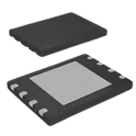
W25Q128JVPIQ
SPI Flash Memory with Dual/Quad SPI The W25Q128JV (128M-bit) Serial Flash memory provides a storage solution for systems with limited space, pins and power. The 25Q series offers flexibility and performance well beyond ordinary Serial Flash devices. They are ideal for code shadowing to RAM, executing code directly from Dual/Quad SPI (XIP) and storing voice, text and data. The device operates on a single 2.7V to 3.6V power supply with current consumption as low as 1µA for power-down. All devices are offered in space-saving packages. The W25Q128JV array is organized into 65,536 programmable pages of 256-bytes each. Up to 256 bytes can be programmed at a time. Pages can be erased in groups of 16 (4KB sector erase), groups of 128 (32KB block erase), groups of 256 (64KB block erase) or the entire chip (chip erase). The W25Q128JV has 4,096 erasable sectors and 256 erasable blocks respectively. The small 4KB sectors allow for greater flexibility in applications that require data and parameter storage. (See Figure 2.) The W25Q128JV supports the standard Serial Peripheral Interface (SPI), Dual/Quad I/O SPI: Serial Clock, Chip Select, Serial Data I/O0 (DI), I/O1 (DO), I/O2 and I/O3. SPI clock frequencies of W25Q128JV of up to 133MHz are supported allowing equivalent clock rates of 266MHz (133MHz x 2) for Dual I/O and 532MHz (133MHz x 4) for Quad I/O when using the Fast Read Dual/Quad I/O. These transfer rates can outperform standard Asynchronous 8 and 16-bit Parallel Flash memories. New Family of SpiFlash Memories – W25Q128JV: 128M-bit / 16M-byte – Standard SPI: CLK, /CS, DI, DO – Dual SPI: CLK, /CS, IO0, IO1 – Quad SPI: CLK, /CS, IO0, IO1, IO2, IO3 – Software & Hardware Reset(1) Highest Performance Serial Flash – 133MHz Single, Dual/Quad SPI clocks – 266/532MHz equivalent Dual/Quad SPI – 66MB/S continuous data transfer rate – Min. 100K Program-Erase cycles per sector – More than 20-year data retention Efficient “Continuous Read” – Continuous Read with 8/16/32/64-Byte Wrap – As few as 8 clocks to address memory – Allows true XIP (execute in place) operation Low Power, Wide Temperature Range – Single 2.7 to 3.6V supply – <1µA Power-down (typ.) – -40°C to +85°C operating range – -40°C to +105°C operating range Flexible Architecture with 4KB sectors – Uniform Sector/Block Erase (4K/32K/64K-Byte) – Program 1 to 256 byte per programmable page – Erase/Program Suspend & Resume Advanced Security Features – Software and Hardware Write-Protect – Power Supply Lock-Down – Special OTP protection – Top/Bottom, Complement array protection – Individual Block/Sector array protection – 64-Bit Unique ID for each device – Discoverable Parameters (SFDP) Register – 3X256-Bytes Security Registers with OTP locks – Volatile & Non-volatile Status Register Bits Space Efficient Packaging – 8-pin SOIC 208-mil – 16-pin SOIC 300-mil (additional /RESET pin) – 8-pad WSON 6x5-mm / 8x6-mm – 24-ball TFBGA 8x6-mm (6x4/5x5 ball array) – 24-ball WLCSP – Contact Winbond for KGD and other options #CommonPartsLibrary #IntegratedCircuit #Memory
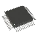
75 Uses0 StarsSTM32L031K6T6TR
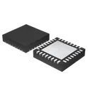
ST Microelectronics STM32L031K6T6TR LQFP-32_L7.0-W7.0-P0.80-LS9.0-BL LCSC Part Number: C2054289 JLCPCB Part Class: Extended Part Manufactured by ST(意法半导体) STMicroelectronics STM32L031x4/6 ultra-low-power 32-bit ARM Cortex-M0+ microcontroller family, operating up to 32MHz, with up to 32KB Flash memory, 1KB EEPROM and 8KB SRAM. Features 12-bit ADC with hardware oversampling, ultra-low-power comparators, timers, RTC, watchdogs, SysTick, I2C, SPI, USART and low-power UART interfaces. Supports multiple internal/external clock sources, low-power modes, backup registers and operation from 1.8V to 3.6V supply, with power-down operation down to 1.65V. Suitable for low-power embedded, battery-powered, sensor, industrial and portable applications. Search Keywords: STM32L031x4, STM32L031x6, STM32L031, STMicroelectronics STM32L031, STM32L031 MCU, STM32L0 microcontroller, ARM Cortex-M0+ MCU, ultra low power STM32, 32MHz microcontroller, STM32 32KB Flash, STM32 EEPROM MCU, STM32L031 I2C SPI USART, STM32L031 low power UART, STM32L031 ADC, STM32L031 datasheet Hashtags: #STM32L031 #STM32L031x4 #STM32L031x6 #STMicroelectronics #STM32L0 #CortexM0Plus #ARMMicrocontroller #UltraLowPowerMCU #32MHzMCU #32KBFlash #EEPROMMCU #I2CMCU #SPIMCU #USARTMCU #LowPowerUART #ADC12bit
52 Uses0 StarsSD-111S
Standard SD card socket with a push-push insertion/ejection mechanism for removable SD memory cards. Surface-mount design with 9 contacts, 2.82 mm height above the PCB, and an operating temperature range of -20°C to +60°C; suitable for embedded systems, consumer electronics, and other compact devices requiring removable storage. #SDCardSocket #MemoryConnector #PushPush #SMD #HanboElectronic
10 Uses0 StarsESP32-S3FH4R2
2.4GHz Wi-Fi+Bluetooth LE SoC ESP32-S3FH4R2 is a highly integrated low-power Wi-Fi and Bluetooth LE System-on-Chip (SoC) from Espressif Systems. It is based on a dual-core Xtensa® LX7 processor running at up to 240 MHz and is designed for IoT, smart home, industrial control, AIoT, audio processing, and embedded applications. The ESP32-S3FH4R2 variant includes 4 MB of in-package Quad SPI Flash and 2 MB of in-package Quad SPI PSRAM, reducing external component count and simplifying PCB design. Key Features Dual-core Xtensa® LX7 CPU Up to 240 MHz operating frequency 32-bit architecture with floating-point unit (FPU) SIMD instructions for AI and signal-processing workloads Integrated Memory 4 MB in-package Flash 2 MB in-package PSRAM 512 KB on-chip SRAM 384 KB ROM Additional RTC memory for low-power operation Wireless Connectivity IEEE 802.11 b/g/n 2.4 GHz Wi-Fi Bluetooth® 5 Low Energy (LE) Long-range and low-power wireless communication support Rich Peripheral Set Up to 45 programmable GPIOs USB OTG and USB Serial/JTAG SPI, I²C, I²S, UART, SDIO TWAI® (CAN 2.0 compatible) Camera interface LCD interface PWM, pulse counter, RMT, DMA controller Analog Features Two 12-bit SAR ADCs Temperature sensor 14 capacitive touch sensing inputs Security Features Secure Boot Flash Encryption AES, SHA, RSA, HMAC hardware accelerators True Random Number Generator (RNG) Digital Signature peripheral Low-Power Operation Multiple power-saving modes ULP-RISC-V coprocessor ULP-FSM coprocessor Deep-sleep support with RTC memory retention
31 Uses0 StarsESP32-S3-MINI-1-N8
ESP32-S3-MINI-1-N8 is a compact, low-power Wi-Fi and Bluetooth module from Espressif Systems based on the ESP32-S3 SoC. It integrates a dual-core Xtensa LX7 processor, 8 MB flash memory, crystal oscillator, RF matching circuitry, and a PCB antenna in a small SMD package, making it ideal for IoT devices, smart home products, industrial automation, HMI applications, AIoT edge devices, and USB-connected embedded systems. Key Features Dual-core 32-bit Xtensa LX7 CPU Up to 240 MHz operating frequency Includes single-precision floating-point unit (FPU) for enhanced processing performance. Integrated Memory 8 MB Quad SPI Flash (N8 variant) 512 KB SRAM 384 KB ROM 16 KB RTC SRAM. Wireless Connectivity 2.4 GHz Wi-Fi 4 (802.11 b/g/n) Data rates up to 150 Mbps Bluetooth 5 LE with Bluetooth Mesh support Simultaneous Wi-Fi and Bluetooth operation through an integrated coexistence mechanism. Rich Peripheral Set Up to 39 GPIOs USB 2.0 OTG USB Serial/JTAG SPI, I²C, I²S, UART PWM, MCPWM SDIO Host ADC Touch sensing Temperature sensor TWAI® (CAN 2.0 compatible) Timers and watchdogs. Integrated Components On-board 40 MHz crystal oscillator PCB antenna RF matching network Compact certified module design. Operating Conditions Supply voltage: 3.0 V to 3.6 V Operating temperature: −40°C to +85°C. Compliance RoHS and REACH compliant RF-certified module for simplified product development. #RF_transceiver #Module #Esp32
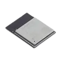
768 Uses0 StarsESP32-WROOM-32UE-N16
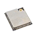
2.4GHz -98dBm SMD,19.2x18mm RF Transceiver Modules and Modems RoHS The ESP32-WROOM-32UE-N16 is a 2.4 GHz wireless MCU module built around the ESP32 SoC. It combines a dual-core processor, integrated Wi-Fi (802.11 b/g/n) and Bluetooth 4.2 (Classic + BLE), along with rich peripherals. The “UE” variant specifically uses a U.FL / IPEX connector for an external antenna, making it ideal for applications that require better RF performance or flexible antenna placement (e.g., enclosed products or long-range communication). The “N16” indicates 16 MB external flash memory, suitable for large firmware, OTA updates, and data-heavy applications. Processing Dual-core Xtensa LX6 32-bit CPU Clock speed up to 240 MHz Memory 16 MB Flash (N16 variant) ~520 KB SRAM + 448 KB ROM Connectivity Wi-Fi: 802.11 b/g/n (up to 150 Mbps) Bluetooth: v4.2 (BR/EDR + BLE) Frequency: 2.4 GHz band Antenna External antenna via U.FL connector Better range and flexibility vs PCB antenna Interfaces / Peripherals GPIO (≈26 usable pins) UART, SPI, I2C, I2S, SDIO ADC, DAC PWM (LED & motor control) Capacitive touch sensing Security Hardware encryption: AES, SHA, RSA Secure boot & flash encryption support Power Operating voltage: 3.0V – 3.6V (typ. 3.3V) Multiple low-power modes for battery applications Environmental Operating temperature: -40°C to +85°C Physical Surface-mount module (~38 pins / 52 pads depending on reference) Compact and RF-shielded design Typical Applications Smart home devices (IoT) Industrial automation Wireless sensors and data loggers Wearables and consumer electronics Remote monitoring systems #Module #ESP32
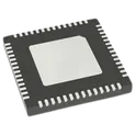
51 Uses0 StarsNRF52832-QFAA-R7
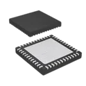
IC RF TxRx + MCU Bluetooth Bluetooth v5.3 2.4GHz 48-VFQFN Exposed Pad NRF52832-QFAA-R7 is an ultra-low-power wireless System-on-Chip (SoC) from Nordic Semiconductor, designed for Bluetooth Low Energy (BLE), ANT, NFC, and proprietary 2.4 GHz wireless applications. It integrates a high-performance ARM Cortex-M4F processor, memory, peripherals, and a 2.4 GHz radio into a single chip, making it ideal for IoT devices, wearables, wireless sensors, beacons, and smart peripherals. GHz protocols • 2.4 GHz transceiver • -96 dBm sensitivity in Bluetooth® low energy mode • Supported data rates: 1 Mbps, 2 Mbps Bluetooth® low energy mode • -20 to +4 dBm TX power, configurable in 4 dB steps • On-chip balun (single-ended RF) • 5.3 mA peak current in TX (0 dBm) • 5.4 mA peak current in RX • RSSI (1 dB resolution) • ARM® Cortex®-M4 32-bit processor with FPU, 64 MHz • 215 EEMBC CoreMark® score running from flash memory • 58 μA/MHz running from flash memory • 51.6 μA/MHz running from RAM • Data watchpoint and trace (DWT), embedded trace macrocell (ETM), and instrumentation trace macrocell (ITM) • Serial wire debug (SWD) • Trace port • Flexible power management • 1.7 V–3.6 V supply voltage range • Fully automatic LDO and DC/DC regulator system • Fast wake-up using 64 MHz internal oscillator • 0.3 μA at 3 V in System OFF mode • 0.7 μA at 3 V in System OFF mode with full 64 kB RAM retention • 1.9 μA at 3 V in System ON mode, no RAM retention, wake on RTC • Memory • 512 kB flash/64 kB RAM • 256 kB flash/32 kB RAM • Nordic SoftDevice ready • Support for concurrent multi-protocol • Type 2 near field communication (NFC-A) tag with wakeup-on-field and touchto-pair capabilities • 12-bit, 200 ksps ADC - 8 configurable channels with programmable gain • 64 level comparator • 15 level low power comparator with wakeup from System OFF mode • Temperature sensor • 32 general purpose I/O pins • 3x 4-channel pulse width modulator (PWM) unit with EasyDMA • Digital microphone interface (PDM) • 5x 32-bit timer with counter mode • Up to 3x SPI master/slave with EasyDMA • Up to 2x I2C compatible 2-wire master/slave • I2S with EasyDMA • UART (CTS/RTS) with EasyDMA • Programmable peripheral interconnect (PPI) • Quadrature decoder (QDEC) • AES HW encryption with EasyDMA • Autonomous peripheral operation without CPU intervention using PPI and EasyDMA • 3x real-time counter (RTC) • Single crystal operation • Package variants • QFN48 package, 6 × 6 mm • WLCSP package, 3.0 × 3.2 mm #CommonPartsLibrary #IntegratedCircuit
52 Uses0 StarsTMP117AIDRVR
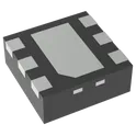
High-Accuracy, Low-Power, Digital Temperature Sensor With SMBus- and I2C-Compatible Interface The TMP117 is a high-precision digital temperature sensor. It is designed to meet ASTM E1112 and ISO 80601 requirements for electronic patient thermometers. The TMP117 provides a 16-bit temperature result with a resolution of 0.0078 °C and an accuracy of up to ±0.1 °C across the temperature range of –20 °C to 50 °C with no calibration. The TMP117 has in interface that is I 2C- and SMBus™-compatible, programmable alert functionality, and the device can support up to four devices on a single bus. Integrated EEPROM is included for device programming with an additional 48-bits memory available for general use. The low power consumption of the TMP117 minimizes the impact of self-heating on measurement accuracy. The TMP117 operates from 1.7 V to 5.5 V and typically consumes 3.5 μA. For non-medical applications, the TMP117 can serve as a single chip digital alternative to a Platinum RTD. The TMP117 has an accuracy comparable to a Class AA RTD, while only using a fraction of the power of the power typically needed for a PT100 RTD. The TMP117 simplifies the design effort by removing many of the complexities of RTDs such as precision references, matched traces, complicated algorithms, and calibration. The TMP117 units are 100% tested on a production setup that is NIST traceable and verified with equipment that is calibrated to ISO/IEC 17025 accredited standards. • TMP117 high-accuracy temperature sensor – ±0.1 °C (maximum) from –20 °C to 50 °C – ±0.15 °C (maximum) from –40 °C to 70 °C – ±0.2 °C (maximum) from –40 °C to 100 °C – ±0.25 °C (maximum) from –55 °C to 125 °C – ±0.3 °C (maximum) from –55 °C to 150 °C • Operating temperature range: –55 °C to 150 °C • Low power consumption: – 3.5-μA, 1-Hz conversion cycle – 150-nA shutdown current • Supply range: – 1.7 V to 5.5 V from –55 °C to 70 °C – 1.8 V to 5.5 V from –55 °C to 150 °C • 16-bit resolution: 0.0078°C (1 LSB) • Programmable temperature alert limits • Selectable averaging • Digital offset for system correction • General-purpose EEPROM: 48 bits • NIST traceability • SMBus™, I2C interface compatibility • Medical grade: meets ASTM E1112 and ISO 80601-2-56 • RTDs replacement: PT100, PT500, PT1000 2 Applications • Electronic thermometers • Wireless environmental sensors • Thermostats • Automotive test equipment • Wearable fitness and activity monitors • Cold chain asset tracking • Gas meters and heat meters • Temperature transmitters #CommonPartsLibrary #Sensor
223 Uses0 StarsESP32-C3FH4
The ESP32-C3FH4 is a highly integrated wireless microcontroller designed for Internet of Things, smart devices, industrial automation, consumer electronics, and embedded connectivity applications. It combines a low-power RISC-V processor with integrated Wi-Fi and Bluetooth Low Energy connectivity, providing a cost-effective and secure platform for wireless communication and edge computing. The device incorporates embedded flash memory, advanced security features, low-power operating modes, and a rich set of peripheral interfaces, making it suitable for battery-powered and always-connected systems. Its compact design and comprehensive software ecosystem enable rapid development of connected products while maintaining high reliability and energy efficiency. The ESP32-C3FH4 is widely used in smart sensors, home automation devices, wearable electronics, industrial monitoring systems, wireless control modules, and cloud-connected embedded products. Features Integrated RISC-V microcontroller core Built-in Wi-Fi connectivity Integrated Bluetooth Low Energy support Embedded flash memory Low-power operation for battery-powered applications Hardware cryptographic acceleration Secure boot capability Flash encryption support Multiple GPIO interfaces Integrated UART, SPI, I²C, I²S, PWM, and ADC peripherals Real-time processing capability Wireless networking and cloud connectivity support OTA firmware update support Compact surface-mount package Industrial-grade reliability Electrical Characteristics Wireless microcontroller architecture Integrated RF subsystem Low-power operating modes High-performance embedded processing Secure communication support Multi-protocol wireless connectivity Flexible peripheral expansion capability Optimized power consumption for IoT devices Applications Internet of Things devices Smart home automation Wireless sensor networks Industrial monitoring systems Asset tracking devices Wearable electronics Smart appliances Remote control systems Data acquisition platforms Edge computing applications Connected consumer products Embedded wireless gateways Package Information Surface-mount package Compact footprint for embedded applications Suitable for automated assembly processes Optimized thermal and electrical performance PCB-friendly package design #commonpartslibrary #integratedcircuit #microcontroller #wirelessconnectivity #wifi #bluetoothlowenergy #iot #embeddedsystems #espressif #smartdevices #industrialautomation #edgecomputing #wirelessmodule #internetofthings #electronicsdesign #riscv #embeddedelectronics #lowpowerdesign
174 Uses0 Stars