Memory
STM32U083CCT6
ARM® Cortex®-M0+ STM32U0 Microcontroller IC 32-Bit 56MHz 256KB (256K x 8) FLASH 48-LQFP (7x7) # STM32U083CCT6 ## General Description The STM32U083CCT6 is an ultra-low-power microcontroller from STMicroelectronics based on the Arm Cortex-M0+ core. It is specifically designed for energy-efficient embedded applications requiring long battery life, advanced peripheral integration, secure operation, and reliable real-time performance. The device combines low-power processing, embedded Flash memory, SRAM, analog peripherals, communication interfaces, and hardware security features within a compact package. Its architecture makes it ideal for smart sensors, industrial monitoring systems, medical devices, wearable electronics, smart metering, home automation products, and Internet of Things applications where power efficiency is a primary design requirement. ## Key Features ### Processing Architecture * Arm Cortex-M0+ processor core * Optimized low-power computing architecture * Efficient real-time processing capability * Interrupt-driven operation support * Embedded system control functionality ### Memory Resources * Embedded Flash memory * Integrated SRAM * Non-volatile data storage support * High-reliability memory architecture * Efficient code execution capability ### Low-Power Features * Ultra-low-power operating modes * Multiple sleep and standby modes * Fast wake-up capability * Battery-powered application optimization * Energy-efficient peripheral operation * Extended product operating life in portable systems ### Security Features * Hardware security mechanisms * Memory protection functionality * Secure firmware execution support * Data integrity protection * Secure embedded application development support ### Communication Interfaces * USART communication interfaces * UART communication support * SPI serial communication interfaces * I²C communication interfaces * Low-power communication capability * Flexible external device connectivity ### Analog Features * Analog-to-digital conversion capability * Precision signal acquisition support * Integrated analog peripherals * Sensor interface compatibility * Low-power analog operation ### Timer and Control Functions * General-purpose timers * PWM signal generation * Real-time clock functionality * Event-driven control capability * Timing and scheduling support ### Package Characteristics * Surface-mount package * Compact footprint design * Automated assembly compatibility * Suitable for space-constrained applications * Industrial-grade packaging ### Material Construction * Advanced low-power semiconductor technology * RoHS-compliant materials * Lead-free package construction * High-reliability integrated circuit design ### Environmental Characteristics * Suitable for industrial and commercial environments * Long operational service life * Stable performance under continuous operation * Robust low-power architecture ### Application Areas * Internet of Things Devices * Smart Sensors * Wearable Electronics * Medical Monitoring Equipment * Home Automation Systems * Smart Metering Applications * Battery-Powered Products * Environmental Monitoring Systems * Industrial Data Acquisition Equipment * Consumer Electronics * Portable Embedded Systems * Wireless Sensor Nodes ### Compliance * RoHS Compliant * Lead-Free Compatible * Industrial-Grade Embedded Microcontroller Solution ## Manufacturer STMicroelectronics ## Product Family STM32U0 Ultra-Low-Power Microcontroller Series #STM32U083CCT6 #STM32U0 #STMicroelectronics #Microcontroller #UltraLowPowerMCU #CortexM0Plus #EmbeddedSystems #IoT #SmartSensors #WearableElectronics #BatteryPoweredDevices #IndustrialElectronics #EmbeddedDesign #FirmwareDevelopment #ElectronicsEngineering
0 Uses
0 Stars
STM32H573ZIT6
ARM® Cortex®-M33 STM32H5 Microcontroller IC 32-Bit 250MHz 2MB (2M x 8) FLASH 144-LQFP (20x20) # STM32H573ZIT6 ## General Description The STM32H573ZIT6 is a high-performance microcontroller from STMicroelectronics based on the Arm Cortex-M33 core. It is designed to deliver advanced processing capability, enhanced security, and extensive peripheral integration for industrial, medical, consumer, communications, and embedded control applications. The device combines powerful computational performance with low-power operation, making it suitable for real-time control, edge computing, human-machine interfaces, industrial automation, IoT gateways, motor control systems, and secure connected devices. Integrated security features, high-speed memory architecture, and comprehensive communication interfaces enable the development of robust and scalable embedded solutions. ## Key Features ### Processing Architecture * Arm Cortex-M33 processor core * TrustZone security architecture * Digital signal processing capabilities * Floating-point computation support * Optimized real-time processing performance ### Memory Resources * Embedded Flash memory * Integrated SRAM architecture * Error correction capability for enhanced reliability * High-speed memory access structure ### Security Features * Secure boot functionality * Hardware cryptographic accelerators * Secure firmware update support * Memory protection mechanisms * Tamper detection capabilities * Trusted execution environment * Secure key management support ### Communication Interfaces * USART and UART communication interfaces * SPI serial communication interfaces * I²C communication interfaces * CAN FD connectivity * USB connectivity support * Ethernet interface capability * SDMMC memory card interface * Flexible external communication options ### Analog Features * High-performance analog-to-digital conversion * Digital-to-analog conversion capability * Analog comparators * Precision signal acquisition support ### Timer and Control Functions * Advanced control timers * General-purpose timers * PWM generation capability * Encoder interface support * Motor-control functionality * Real-time clock integration ### Power Characteristics * Low-power operating modes * Dynamic power optimization * Battery-powered application support * Efficient performance-to-power ratio ### Package Characteristics * LQFP package construction * Surface-mount technology compatibility * Industrial-grade mechanical design * Suitable for automated assembly processes ### Application Areas * Industrial Automation Systems * Motor Control Equipment * Human-Machine Interfaces * Smart Energy Systems * Medical Electronics * IoT Gateways * Secure Embedded Devices * Industrial Networking Equipment * Building Automation Systems * Consumer Electronics * Data Acquisition Systems * Edge Computing Applications ### Compliance * RoHS Compliant * Lead-Free Compatible * Industrial and Commercial Application Support ## Manufacturer STMicroelectronics ## Product Family STM32H5 Series High-Performance Microcontrollers #STM32H573ZIT6 #STM32H5 #STMicroelectronics #CortexM33 #Microcontroller #EmbeddedSystems #IndustrialAutomation #SecureMCU #IoT #EdgeComputing #MotorControl #EmbeddedDesign #ElectronicsEngineering #FirmwareDevelopment #IndustrialElectronics
0 Uses
0 Stars
W25Q128JVSIM
FLASH - NOR Memory IC 128Mb (16M x 8) SPI - Quad I/O, QPI, DTR 133 MHz 8-SOIC 128M-bit Serial Flash Memory with uniform 4KB sectors and Dual/Quad SPI Winbond W25Q128JV is a 128-Mbit (16 MB) serial NOR Flash memory device designed for code and data storage in embedded systems. It supports standard SPI, Dual SPI, Quad SPI (QSPI), and Dual/Quad Peripheral Interface (DPI/QPI) modes, enabling high-speed data transfer rates up to 133 MHz clock operation and up to 532 MB/s equivalent throughput in Quad I/O DTR mode. The device supports Execute-In-Place (XIP), allowing processors and microcontrollers to run code directly from external flash memory without copying it to RAM. Features include 4 KB sector erase, 32 KB and 64 KB block erase, page programming, hardware/software write protection, security registers, JEDEC identification, SFDP support, suspend/resume operations, and low-power standby modes. Suitable for microcontrollers, FPGA configuration storage, IoT devices, industrial controllers, networking equipment, consumer electronics, and embedded systems requiring reliable non-volatile memory. Search Keywords: W25Q128JV, Winbond flash memory, SPI NOR Flash, QSPI Flash, Quad SPI memory, Serial Flash memory, 128Mbit Flash, 16MB Flash memory, Execute In Place XIP, external MCU flash, ESP32 flash memory, FPGA configuration memory, NOR flash storage, W25Q128, Dual SPI Flash, Quad I/O Flash, embedded nonvolatile memory, serial flash IC Hashtags: #W25Q128JV #Winbond #NORFlash #SPIMemory #QSPI #SerialFlash #FlashMemory #EmbeddedSystems #Microcontroller #ESP32 #FPGA #NonVolatileMemory #XIP #IoT #ElectronicsDesign #MemoryIC #FirmwareStorage #QuadSPI #EmbeddedHardware #ElectronicComponents
15 Uses
0 Stars
W55RP20
Ethernet ICs W55RP20 microcontroller, Dual ARM Cortex-M0+ a. 133MHz, 2MByte Flash memory on-chip, 264kB on-chip SRAM in six independent banks, DMA controller W55RP20 is a highly integrated System-in-Package (SiP) from WIZnet that combines the popular RP2040 dual-core microcontroller with a W5500 hardware TCP/IP Ethernet controller. Designed for IoT, industrial automation, and embedded networking applications, the W55RP20 delivers reliable Ethernet connectivity, low power consumption, and high-performance processing in a compact package. It simplifies Ethernet-enabled designs by integrating the MCU, network stack, flash memory, and Ethernet functionality into a single device. Key Features Dual-core ARM Cortex-M0+ processor running up to 133 MHz Integrated hardwired TCP/IP stack for reliable Ethernet communication 2 MB on-chip Flash memory 264 KB SRAM in six independent memory banks Built-in 10BASE-T / 100BASE-TX Ethernet MAC and PHY Supports TCP, UDP, IPv4, ICMP, ARP, IGMP, and PPPoE protocols 23 GPIO pins, including 4 analog-capable inputs 2× UART, 2× SPI, and 2× I²C interfaces 16 PWM channels and 8 Programmable I/O (PIO) state machines USB 1.1 Host/Device controller with integrated PHY 12-channel DMA controller for efficient data transfer Operating voltage range of 1.8 V to 3.3 V Industrial temperature support up to -40°C to +85°C Compact 68-QFN package for space-constrained designs #W55RP20 #WIZnet #RP2040 #EthernetMCU #IoT #EmbeddedSystems #IndustrialAutomation #TCPIP #EthernetController #Microcontroller #HardwareTCPIP #Networking #EmbeddedDesign #SmartDevices #IoTDevelopment
1 Use
0 Stars
NRF54L15-CAAA-R7
IC RF TxRx + MCU 802.15.4, Bluetooth Bluetooth v5.4, Matter, Thread, Zigbee® 47-XFBGA, WLCSP # NRF54L15-CAAA-R7 ## General Description The NRF54L15-CAAA-R7 is an ultra-low-power wireless System-on-Chip (SoC) developed by [Nordic Semiconductor](https://www.nordicsemi.com?utm_source=chatgpt.com) for advanced Internet of Things (IoT), industrial, medical, smart home, and wireless sensing applications. The device integrates a high-performance Arm Cortex-M33 processor, a dedicated RISC-V coprocessor, large embedded memory resources, and a multiprotocol 2.4 GHz radio subsystem into a compact package. It is designed to provide exceptional energy efficiency, robust wireless connectivity, and enhanced security while supporting modern wireless standards including Bluetooth® Low Energy, Matter, Thread, Zigbee®, Bluetooth Mesh, Amazon Sidewalk, and proprietary 2.4 GHz protocols. The device is optimized for battery-powered applications requiring extended operating life, high processing capability, and scalable connectivity solutions. ## Key Features ### Processing Architecture * 128 MHz Arm® Cortex®-M33 application processor * Integrated 128 MHz RISC-V coprocessor * TrustZone® security architecture ### Memory Resources * 1.5 MB Non-Volatile Memory (NVM) * 256 KB RAM ### Wireless Connectivity * Multiprotocol 2.4 GHz RF transceiver * Bluetooth® Low Energy support * Matter support * Thread support * Zigbee® support * Bluetooth Mesh support * Amazon Sidewalk support * Proprietary 2.4 GHz protocol support * Bluetooth Channel Sounding capability * Compatible with Wi-Fi companion devices ### RF Performance * Data rates up to 4 Mbps * Output power up to +8 dBm * High receiver sensitivity for extended wireless range ### Security Features * Hardware cryptographic engine * Side-channel attack protection * Tamper detection mechanisms * Secure boot and secure firmware update support ### Peripheral Interfaces * SPI * I²C (TWI) * UART * I²S * GPIO * ADC * PWM * PDM * NFC * QDEC ### Power Characteristics * Ultra-low-power operation * Optimized sleep modes * Battery-powered application support * Operating supply voltage from 1.7 V to 3.6 V ### Package Information * WLCSP package * Surface-mount technology * Industrial operating temperature support ## Applications * Smart Home Devices * Industrial IoT Systems * Wearable Electronics * Medical and Healthcare Devices * Asset Tracking Solutions * Wireless Sensors * Building Automation Systems * Smart Lighting Controls * Consumer Electronics * Connected Peripheral Devices #NordicSemiconductor #nRF54L15 #NRF54L15CAAAR7 #BluetoothLE #Matter #Thread #Zigbee #IoT #WirelessSoC #EmbeddedSystems #IndustrialIoT #SmartHome #LowPowerDesign #CortexM33 #RISCV
1 Use
0 Stars
STM32MP157CAC3
ARM® Cortex®-A7 Microprocessor IC STM32MP1 2 Core, 32-Bit 209MHz, 650MHz 361-TFBGA (12x12) # Engineering Specification ## Product Name STM32MP157CAC3 ## General Description STM32MP157CAC3 is a high-performance microprocessor unit that combines application processing and real-time control capabilities within a single integrated circuit. The device is designed to support advanced embedded systems requiring a balance of computing performance, deterministic control, multimedia processing, connectivity, and security functionality. The component integrates multi-core processing resources, memory interfaces, graphics capabilities, peripheral controllers, and communication subsystems to enable the development of sophisticated embedded platforms. Its heterogeneous architecture allows high-level operating systems and real-time firmware to operate simultaneously, supporting applications that require both user-interface functionality and low-latency control. The device is intended for industrial automation, human-machine interface systems, edge computing platforms, communication equipment, medical devices, smart infrastructure, and Internet of Things applications. Its architecture enables consolidation of system functions, reducing component count and simplifying overall hardware design. The design emphasizes processing efficiency, system scalability, power management, security, and long-term reliability. It supports advanced software ecosystems and facilitates the development of connected embedded products with graphical interfaces, networking capabilities, and real-time operational control. ## Functional Requirements ### Application Processing The device shall provide application-level processing capabilities suitable for operating systems, middleware, and user applications. ### Real-Time Processing The device shall support deterministic control functions for time-critical embedded operations. ### Multimedia Support The component shall support graphical and multimedia processing functions for display and user-interface applications. ### System Integration The device shall integrate processing, communication, and peripheral functions within a unified embedded computing platform. ## Electrical Requirements ### Power Management The device shall support efficient power operation and multiple power management modes to optimize energy consumption. ### Memory Interface Support The component shall support external memory devices for program execution, data storage, and system operation. ### Peripheral Connectivity The device shall provide interfaces for communication, control, monitoring, and external subsystem integration. ### Signal Integrity The design shall support reliable operation across supported interface standards and operating conditions. ## Processing Architecture Requirements ### Multi-Core Operation The device shall support concurrent execution of application and real-time workloads through integrated processing resources. ### Operating System Support The architecture shall support embedded operating systems and software frameworks suitable for advanced application development. ### Security Features The device shall support hardware-based mechanisms intended to protect system integrity, software assets, and sensitive data. ### Resource Management The component shall support efficient allocation of processing, memory, and peripheral resources. ## Mechanical Requirements ### Surface Mount Construction The device shall be supplied in a high-density surface mount package suitable for automated manufacturing processes. ### PCB Integration The package shall support integration into multilayer printed circuit boards designed for high-performance embedded systems. ### Structural Integrity The device shall maintain electrical and mechanical reliability during assembly and operational service life. ## Environmental Requirements ### Operating Conditions The component shall operate reliably within environmental conditions commonly encountered in industrial and embedded applications. ### Thermal Performance The device shall support stable operation under sustained processing workloads and associated thermal conditions. ### Storage and Handling The component shall maintain physical and electrical integrity during transportation, storage, and manufacturing processes. ## Quality Requirements ### Reliability The device shall provide dependable long-term operation in embedded and industrial computing environments. ### Verification Processing, peripheral, communication, and system functions shall be validated through applicable testing and qualification procedures. ### Compliance The product shall conform to relevant semiconductor, quality, and embedded computing standards applicable to its intended use. ## Documentation Requirements Technical documentation shall include processor architecture information, hardware integration guidelines, memory interface recommendations, power management considerations, software development support, security features, and application design guidance. ## Classification Tags #STM32MP157CAC3 #STM32MP1 #Microprocessor #MPU #EmbeddedProcessor #ARMProcessor #EmbeddedLinux #RealTimeControl #IndustrialAutomation #HumanMachineInterface #EdgeComputing #IoTGateway #EmbeddedSystems #SystemOnChip #SoC #ApplicationProcessor #GraphicsProcessor #ConnectivityPlatform #IndustrialElectronics #PCBDesign #HardwareDevelopment #ElectricalEngineering #CommonPartsLibrary #ComponentLibrary #EngineeringSpecification #TechnicalDocumentation #SystemIntegration #SecureEmbeddedSystems #MulticoreProcessing
2 Uses
0 Stars
Z84C2006PEG
Interface - Specialized Z84C2006PEG PDIP-40_L52.3-W13.8-P2.54-LS15.2-BL LCSC Part Number: C2614542 JLCPCB Part Class: Extended Part Manufactured by Zilog Z84C00 / Z84C0008PEC PDIP-40 Zilog Z80 microprocessor family, fourth-generation enhanced 8-bit CPU architecture with high computational performance and efficient memory utilization. Features two complete sets of general-purpose registers (main and alternate register banks) for fast context switching, two 16-bit index registers (IX and IY), stack pointer, program counter, refresh register, and interrupt register. Supports a single +5V power supply and interfaces directly with standard memory and peripheral devices. Includes advanced interrupt handling, daisy-chain interrupt capability, and built-in dynamic RAM refresh support. Widely used in industrial control systems, embedded equipment, terminals, instrumentation, retro computers, and communication devices. Search Keywords: Z80 CPU, Zilog Z80, Z84C00, Z8400, 8-bit microprocessor, enhanced Z80 processor, DIP40 CPU, CMOS Z80, NMOS Z80, embedded processor, industrial controller CPU, retro computer processor, vintage microprocessor, dynamic RAM refresh CPU, interrupt controller compatible CPU Hashtags: #Z80 #Zilog #Z84C00 #Z8400 #8BitCPU #Microprocessor #EmbeddedSystems #IndustrialElectronics #RetroComputing #VintageComputing #DIP40 #ComputerArchitecture #DigitalElectronics #CPU #ClassicComputing
0 Uses
0 Stars
Z84C0006PEG
Zilog Z80 microprocessor family, fourth-generation enhanced 8-bit CPU architecture with high computational performance and efficient memory utilization. Features two complete sets of general-purpose registers (main and alternate register banks) for fast context switching, two 16-bit index registers (IX and IY), stack pointer, program counter, refresh register, and interrupt register. Supports a single +5V power supply and interfaces directly with standard memory and peripheral devices. Includes advanced interrupt handling, daisy-chain interrupt capability, and built-in dynamic RAM refresh support. Widely used in industrial control systems, embedded equipment, terminals, instrumentation, retro computers, and communication devices. Search Keywords: Z80 CPU, Zilog Z80, Z84C00, Z8400, 8-bit microprocessor, enhanced Z80 processor, DIP40 CPU, CMOS Z80, NMOS Z80, embedded processor, industrial controller CPU, retro computer processor, vintage microprocessor, dynamic RAM refresh CPU, interrupt controller compatible CPU Hashtags: #Z80 #Zilog #Z84C00 #Z8400 #8BitCPU #Microprocessor #EmbeddedSystems #IndustrialElectronics #RetroComputing #VintageComputing #DIP40 #ComputerArchitecture #DigitalElectronics #CPU #ClassicComputingMicroprocessors - MPU 6MHz Z80 CMOS CPU XT
2 Uses
0 Stars
MCP4461-103E/ST
Digital Potentiometer 10k Ohm 4 Circuit 257 Taps I2C Interface 20-TSSOP # Engineering Specification ## Product Name MCP4461-103E/ST ## General Description MCP4461-103E/ST is a non-volatile digital potentiometer integrated circuit designed to provide electronically programmable resistance adjustment for analog and mixed-signal applications. The device enables precise digital control of resistance values through a serial communication interface, eliminating the need for manual potentiometer adjustments and enhancing system automation capabilities. The component integrates multiple resistor networks, non-volatile memory, and digital control logic within a compact package, making it suitable for signal conditioning, gain adjustment, calibration, offset trimming, volume control, and configuration management applications. The design supports reliable operation in embedded systems, industrial electronics, instrumentation equipment, communication devices, and consumer products requiring programmable analog control. The device is optimized for ease of integration, low power consumption, repeatable performance, and long-term reliability. Non-volatile memory functionality allows resistance settings to be retained during power interruptions, supporting consistent system behavior and simplified startup configuration. ## Functional Requirements ### Digital Resistance Control The device shall provide programmable resistance adjustment through a digital communication interface. ### Non-Volatile Memory Operation The device shall retain programmed resistance settings when power is removed and restore stored values upon power-up. ### Multi-Channel Adjustment The device shall support independent control of multiple resistance channels for flexible system configuration. ### Analog Signal Conditioning The device shall support use in gain control, calibration, bias adjustment, offset correction, and signal tuning applications. ## Electrical Requirements ### Power Supply Compatibility The device shall operate from standard low-voltage electronic power supply rails suitable for embedded and industrial systems. ### Digital Communication The device shall support serial communication for configuration, programming, and control of internal resistance networks. ### Resistance Network Performance The device shall provide repeatable and stable resistance adjustment characteristics throughout normal operating conditions. ### Low Power Operation The device shall minimize power consumption while maintaining functional performance and memory retention capability. ### Noise and Signal Integrity The design shall support accurate analog signal processing with minimal impact on system performance. ## Mechanical Requirements ### Package Construction The component shall be supplied in a surface-mount package suitable for automated PCB assembly processes. ### Board Integration The device shall support standard printed circuit board mounting practices and electronic manufacturing workflows. ### Structural Reliability The package shall maintain electrical and mechanical integrity during handling, assembly, and operational service. ## Environmental Requirements ### Operating Environment The device shall operate reliably within environmental conditions commonly encountered in commercial and industrial electronic equipment. ### Storage Conditions The component shall maintain functional and physical integrity during storage, transportation, and inventory management activities. ### Environmental Robustness The design shall support stable operation under expected temperature and humidity variations within specified application environments. ## Quality Requirements ### Reliability The device shall provide consistent long-term performance with stable resistance characteristics and memory retention capability. ### Verification Electrical functionality, communication performance, memory operation, and resistance adjustment behavior shall be validated through applicable testing procedures. ### Compliance The product shall conform to relevant semiconductor manufacturing, quality assurance, and electronic component standards. ## Documentation Requirements Technical documentation shall include device functionality, communication interface requirements, programming guidelines, application recommendations, electrical characteristics, package information, and reliability considerations. ## Classification Tags #MCP4461 #MCP4461103EST #DigitalPotentiometer #NonVolatileMemory #IntegratedCircuit #ICComponent #AnalogElectronics #MixedSignalDesign #SignalConditioning #GainControl #CalibrationCircuit #EmbeddedSystems #ElectronicComponents #ElectricalEngineering #PCBDesign #CircuitDesign #IndustrialElectronics #Instrumentation #CommonPartsLibrary #EngineeringSpecification #ComponentLibrary #TechnicalDocumentation #SystemIntegration #HardwareDevelopment #ReliabilityEngineering
0 Uses
0 Stars
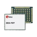
ZED-F9T-00B
ZED-F9T RF Receiver BeiDou, Galileo, GLONASS, GNSS, GPS -167dBm 54-LGA (22x17) Ang ZED-F9T-00B ay isang high-precision multi-band GNSS timing module mula sa u-blox na idinisenyo para sa mga application na nangangailangan ng napakatumpak na time synchronization. Gumagamit ito ng sabay-sabay na pagtanggap ng maraming GNSS constellations kabilang ang GPS, Galileo, BeiDou, at GLONASS upang makapagbigay ng nanosecond-level timing accuracy para sa telecommunications, smart grids, industrial automation, at critical network infrastructure. Ang module ay partikular na angkop para sa 4G/5G network synchronization at iba pang timing-sensitive systems. Key Features Multi-band GNSS receiver para sa high-accuracy timing applications Nanosecond-level timing accuracy (hanggang 5 ns typical timing accuracy) Support para sa GPS/QZSS, Galileo, BeiDou, at GLONASS constellations Differential timing mode para sa mas mataas na timing precision Configurable time pulse output mula 0.25 Hz hanggang 25 MHz Time pulse jitter na hanggang ±4 ns Carrier phase output support Built-in TCXO at programmable flash memory Integrated security features para sa mas mataas na robustness laban sa signal attacks UART, USB, SPI, at I²C communication interfaces Operating temperature range na -40°C hanggang +85°C Compact 17.0 mm × 22.0 mm × 2.4 mm LGA package Dinisenyo upang matugunan ang mahihigpit na 5G timing synchronization requirements #uBlox #ZEDF9T00B #GNSS #GPS #Galileo #BeiDou #GLONASS #TimingModule #HighPrecisionTiming #5G #Telecommunications #NetworkSynchronization #IndustrialAutomation #SmartGrid #LGA #EmbeddedSystems #IoT #ElectronicsDesign #HardwareEngineering #RFModule
1 Use
0 Stars


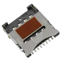
693022010811
8 Position Card Connector Micro SIM Surface Mount, Right Angle Gold ## Engineering Specification ## General Description The **693022010811** is a Würth Elektronik **WR-CRD Micro SIM card connector** designed for compact electronic devices requiring secure SIM card retention and reliable board-level electrical connection. It is intended for surface-mount printed circuit board assembly and is suitable for communication modules, wireless devices, embedded systems, IoT hardware, and networking equipment. The connector uses a hinged lid mechanism to hold the Micro SIM card in place during operation. ## Device Identification Manufacturer Part Number: **693022010811** Manufacturer: **Würth Elektronik** Product Series: **WR-CRD** Device Category: **Connector and Interconnect Component** Device Type: **Micro SIM Card Connector** Connector Style: **Hinge Type** Mounting Type: **Surface Mount, Right Angle** ## Functional Description The device functions as a board-mounted Micro SIM card interface. It provides mechanical retention and electrical contact between the SIM card and the host printed circuit board. The hinged lid design allows the SIM card to be placed into the connector and secured during operation, helping maintain contact stability in compact electronic assemblies. ## Mechanical Description The connector is designed with a low-profile surface-mount construction suitable for space-constrained PCB layouts. It uses a hinged card-retention mechanism and is intended for horizontal or right-angle card installation. The mechanical structure supports reliable insertion, retention, and removal of the Micro SIM card during normal use. ## Electrical Description The connector is intended for signal-level SIM card interface applications. It provides multiple gold-plated contact positions for stable electrical connection between the SIM card and the host circuit. The device should be used within the manufacturer’s specified voltage, current, contact resistance, and insulation limits. ## Material and Contact Description The connector uses copper alloy contacts with gold plating for reliable signal transfer and corrosion resistance. The housing and mechanical retention structure are designed for surface-mount assembly and repeated card handling within the rated operating conditions. ## Mounting and Assembly Description The component is suitable for automated surface-mount PCB assembly. Proper land pattern design, soldering profile control, and mechanical clearance should be followed according to the manufacturer’s recommended layout and assembly guidance. The PCB design should provide stable grounding, correct pad alignment, and adequate clearance for SIM card insertion and lid operation. ## Application Suitability The **693022010811** is suitable for cellular communication devices, IoT modules, wireless routers, embedded modems, tracking systems, smart meters, industrial communication equipment, portable electronics, and other products requiring a Micro SIM card interface. ## Design Considerations The connector should be placed in an accessible area of the PCB to allow SIM card installation and removal. Designers should avoid excessive mechanical stress on the hinged lid, improper solder joint loading, contamination of the contact area, and operation beyond the specified environmental and electrical ratings. ## Hashtags #commonpartslibrary #connector #simconnector #microsimconnector #wurthelektronik #wrcrd #cardconnector #memoryconnector #interconnect #pcbconnector #surfacemount #rightangleconnector #smtcomponent #goldplatedcontacts #embeddedhardware #iotdevices #wirelessmodules #communicationdevices #networkingequipment #pcbdesign #hardwaredesign #electronicscomponents #electronicparts #componentlibrary #engineeringparts #electronicsengineering
0 Uses
0 Stars
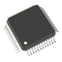
R7FA6E10F2CFM#AA0
ARM® Cortex®-M33 RA6E1 Microcontroller IC 32-Bit 200MHz 1MB (1M x 8) FLASH 64-LFQFP (10x10) ## Engineering Specification ## General Description The **R7FA6E10F2CFM#AA0** is a Renesas Electronics **RA6E1 series microcontroller** designed for embedded control, industrial electronics, IoT edge devices, automation systems, and general-purpose connected applications. It is built around an **Arm Cortex-M33 processor with TrustZone support**, providing high performance, secure execution capability, and flexible integration for modern embedded designs. ## Device Identification Manufacturer Part Number: **R7FA6E10F2CFM#AA0** Manufacturer: **Renesas Electronics** Product Family: **RA Family** Series: **RA6 Series** Group: **RA6E1 Group** Device Category: **Integrated Circuit** Device Type: **Microcontroller Unit** ## Core and Processing The device uses an **Arm Cortex-M33 core** and is intended for high-performance embedded processing. It supports secure application development through TrustZone technology and is suitable for systems requiring reliable control, fast response, and efficient software execution. ## Memory Configuration The microcontroller includes program flash memory, data flash memory, and SRAM resources suitable for embedded firmware, application code, configuration storage, and runtime processing requirements. ## Package and Mechanical Description The component is supplied in an **LQFP surface-mount package**, making it suitable for compact printed circuit board layouts and standard automated assembly processes. ## Electrical and Operating Description The device is designed for low-voltage embedded systems and supports operation across an industrial temperature range. It is suitable for products requiring stable performance in controlled, commercial, or industrial operating environments. ## Communication and Interface Support The device supports common embedded communication interfaces such as USB, UART, SPI, I²C, QSPI, and CAN, allowing integration with sensors, displays, external memory, communication modules, and other peripheral devices. ## Analog and Control Features The microcontroller includes analog conversion capability, timer functions, PWM support, watchdog protection, reset monitoring, and low-voltage detection features. These functions make it suitable for control systems, monitoring equipment, and mixed-signal embedded applications. ## Security and Debug Features The device supports embedded security functions including TrustZone, unique device identification, and true random number generation. Debug and development access is supported through standard JTAG and SWD interfaces. ## Application Suitability This device is suitable for embedded controllers, IoT devices, industrial automation, metering equipment, appliance control, USB-connected products, sensor-based systems, and general electronic control applications requiring a compact and secure microcontroller solution. ## Hashtags #commonpartslibrary #integratedcircuit #microcontroller #renesas #renesaselectronics #ra6e1 #ra6series #armcortexm33 #embeddedsystems #electronicscomponents #semiconductor #mcu #iotdevices #industrialautomation #pcbdesign #electronicparts #componentlibrary #engineeringparts #hardwaredesign #electronicsengineering
0 Uses
0 Stars
MIMXRT1189XVM8C
ARM® Cortex®-M33F, ARM® Cortex®-M7F RT1180 Microcontroller IC 32-Bit Dual-Core 240MHz, 800MHz 160KB (160K x 8) ROM 289-LFBGA (14x14) The MIMXRT1189XVM8C is a high-performance crossover microcontroller from the NXP Semiconductors i.MX RT1180 family, designed for advanced industrial and real-time embedded applications. It combines the real-time performance of a microcontroller with the connectivity and security features typically found in application processors. The device integrates dual Arm® Cortex® cores, high-speed networking with Time-Sensitive Networking (TSN), and advanced EdgeLock® security technology, making it ideal for industrial automation, robotics, motor control, automotive gateways, and Industry 4.0 systems. Key Features Dual-core architecture: Arm® Cortex®-M7 core running up to 800 MHz Arm® Cortex®-M33 core running up to 300 MHz Integrated Gigabit TSN Ethernet switch for deterministic real-time networking Supports industrial Ethernet protocols including: EtherCAT PROFINET Ethernet/IP CC-Link IE Advanced EdgeLock® Secure Enclave for secure boot, cryptography, and tamper detection Up to 1.5 MB on-chip SRAM with ECC protection High-speed external memory interfaces Multiple communication peripherals: CAN-FD UART SPI I2C USB Ethernet High-resolution ADCs and advanced PWM/timer modules Supports MCUXpresso SDK and Zephyr RTOS Industrial temperature range operation from -40°C to +125°C BGA package optimized for compact industrial designs #Commonpartlibrary #Microcontroller #MIMXRT1189
8 Uses
0 Stars
STM32WLE5JCI6
Multiprotocol LPWAN 32-bit Arm Cortex-M4 MCUs, LoRa, (G)FSK, (G)MSK, BPSK, up to 256KB flash, 64KB SRAM IC RF TxRx + MCU 802.15.4 LoRa™ 150MHz ~ 960MHz 73-UFBGA The STM32WLE5JCI6 is an ultra-low-power wireless System-on-Chip (SoC) from STMicroelectronics that combines a 32-bit Arm Cortex-M4 microcontroller with an integrated sub-GHz radio transceiver. It is designed for long-range, low-power IoT and LPWAN applications such as smart metering, smart cities, industrial sensors, and remote monitoring systems. It supports multiple modulation schemes including LoRa®, (G)FSK, (G)MSK, and BPSK, making it flexible for both proprietary and standardized wireless protocols like LoRaWAN®. The device integrates RF, analog, digital, and security features into a single chip to reduce external components and PCB size. Key Features Core & Performance 32-bit Arm® Cortex®-M4 core up to 48 MHz DSP instructions and MPU support Up to 256 KB Flash and 64 KB SRAM Wireless Radio Sub-GHz frequency range: 150 MHz – 960 MHz Supports LoRa®, (G)FSK, (G)MSK, BPSK High receiver sensitivity up to –148 dBm (LoRa mode) Output power up to +22 dBm Ultra-Low Power Operation Supply voltage: 1.8 V – 3.6 V Very low sleep currents (nA–µA range) Optimized for battery-powered and energy-harvesting devices Peripherals Up to 43 GPIOs ADC (12-bit), DAC, comparators Multiple timers (16-bit and 32-bit) Interfaces: SPI, I2C, UART/USART, LPUART, I2S Security Features Hardware AES-256 encryption True Random Number Generator (TRNG) Secure memory protection and unique device ID System Integration Integrated RF + MCU (highly reduced BOM) OTA firmware update capability Industrial temperature range (typically –40°C to +85°C / +105°C depending variant) Summary The STM32WLE5JCI6 is a highly integrated LoRa-capable MCU + RF transceiver SoC, optimized for long-range wireless communication with extremely low power consumption, making it ideal for IoT devices that must run for years on battery power. #CommonPartsLibrary #IntegratedCircuit #STM32WLE5JCI6 #STM32WL #LoRa #IoT #LowPowerMCU #ArmCortexM4 #SubGHzRF #WirelessMCU #LPWAN #STMicroelectronics
0 Uses
0 Stars
STN1110-I/MM
STN1110-IMM General Description The STN1110-IMM is a multiprotocol OBD-II to UART interpreter integrated circuit designed for automotive diagnostic, telematics, and vehicle communication applications. The device translates OBD-II network traffic into a UART serial data stream for communication with external microcontrollers, embedded processors, and host systems. It supports all legislated OBD-II protocols and provides compatibility with ELM327-based software while offering enhanced processing performance, expanded memory resources, advanced message filtering, firmware upgrade capability, and low-power operation. The device is intended for use in automotive diagnostic tools, fleet management systems, vehicle monitoring equipment, data acquisition systems, and embedded automotive communication products. Engineering Specification Part Number: STN1110-IMM Component Type: OBD-II to UART Interpreter Integrated Circuit Device Category: Automotive Communication Interface IC Package Type: QFN Mounting Type: Surface Mount Device (SMD) Interface Type: * UART * OBD-II Supported Protocols: * ISO 15765-4 CAN * ISO 14230-4 KWP2000 * ISO 9141-2 * SAE J1850 PWM * SAE J1850 VPW Key Features: * Multiprotocol OBD-II support * ELM327 command compatibility * Enhanced ST command extensions * High-speed UART communication * Advanced message filtering * Firmware upgrade capability * Large message buffering * Low-power operation * Automotive diagnostic interface functionality Applications: * OBD-II Scan Tools * Vehicle Diagnostics * Automotive Telematics * Fleet Management Systems * Data Logging Equipment * Embedded Automotive Controllers * Emissions Monitoring Systems * Vehicle Communication Gateways Tags #commonpartslibrary #integratedcircuit #ic #automotive #automotiveelectronics #automotivediagnostics #obdii #obd #uart #vehiclecommunication #telematics #embeddedsystems #communicationinterface #diagnosticinterface #scantool #canbus #kwp2000 #saej1850 #iso9141 #surfaceMount #smd #qfn #electroniccomponent #semiconductor #vehicleelectronics #microcontrollerinterface #datalogging #fleetmanagement #embeddedhardware #hardwaredesign
1 Use
0 Stars
A-CCS_068-Z-T
ASSMANN WSW A-CCS 068-Z-T ASSMANN ASSMANN A-CCS 020-Z-T PLCC socket connector, 20-pin through-hole (THT) socket for PLCC integrated circuits, 1.27mm pitch contacts, PPS glass-fiber reinforced UL94V-0 housing, phosphor bronze contacts with matte tin plating over nickel, low insertion force design, rated for 1A and 125–250V operation, 200 mating cycles, operating temperature -40°C to +105°C, designed for removable PLCC memory devices, microcontrollers, programmable logic ICs and development hardware. Search Keywords: A-CCS 020-Z-T, ACCS020ZT, ASSMANN A-CCS 020-Z-T, ASS 0981 CO, PLCC socket 20 pin, 20 pin PLCC socket, PLCC IC socket, 1.27mm pitch PLCC socket, through hole PLCC socket, THT PLCC socket, ASSMANN PLCC socket, removable IC socket, PLCC connector Hashtags: #ACCS020ZT #ASSMANN #PLCCSocket #20PinPLCC #PLCCConnector #ICSocket #ThroughHoleSocket #THTSocket #127mmPitch #EmbeddedHardware #ProgrammableLogic #MicrocontrollerSocket #ElectronicsConnector #SocketConnector
0 Uses
0 Stars
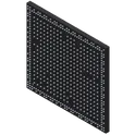
IM8G32L4JCBG-046I
SDRAM - Mobile LPDDR4X Memory IC 8Gbit Parallel 2.133 GHz 200-FBGA (10x15) The IM8G32L4JCBG-046I is an 8Gb (1GB) LPDDR4X SDRAM memory device designed for high-performance, low-power embedded applications. Organized as 256M × 32 bits, it delivers data rates up to 4266 MT/s, making it suitable for industrial computing, AI edge devices, networking equipment, automotive systems, and other memory-intensive applications. The LPDDR4X architecture reduces power consumption while maintaining high bandwidth and reliable operation across industrial temperature ranges. Key Features 8Gb (Gigabit) LPDDR4X SDRAM Memory organization: 256M × 32 bits High-speed operation up to 4266 MT/s Low-power LPDDR4X interface for reduced energy consumption 32-bit data bus width Industrial operating temperature range: –40°C to +95°C 200-ball FBGA package (10 mm × 15 mm) High bandwidth for demanding embedded applications Optimized for low-power and thermally constrained designs Suitable for industrial, automotive, networking, and edge AI systems #LPDDR4X #SDRAM #MemoryIC #EmbeddedSystems #IndustrialElectronics #EdgeComputing #AIoT #HighSpeedMemory #LowPowerDesign #AutomotiveElectronics #NetworkingHardware #FBGA #HardwareDesign #ElectronicsEngineering #PCBDesign #IntelligentMemory
148 Uses
0 Stars
GW2ANR-LV18QN88C8_I7
GW2AR-LV18QN88C8/I7 GOWIN GW2ANR series FPGA, non-volatile Arora family FPGA with integrated SDRAM and NOR Flash, fabricated on 55nm SRAM technology, 1.0V core voltage, low-power architecture with dynamic clock control, high-performance DSP resources, high-speed LVDS interfaces, abundant block SRAM memory, hot-swap support, configurable I/O standards including LVCMOS, LVTTL, SSTL, HSTL, PCI, LVDS and MLVDS, programmable drive strength and pull-up/pull-down options, designed for high-speed, low-cost embedded, industrial, communication and signal-processing applications. Search Keywords: GW2ANR, GOWIN GW2ANR, Arora FPGA, GOWIN FPGA, non volatile FPGA, FPGA with SDRAM, FPGA with NOR Flash, 55nm FPGA, low power FPGA, LVDS FPGA, DSP FPGA, embedded FPGA, GW2ANR series, GOWIN Arora family, programmable logic device Hashtags: #GW2ANR #GOWINGW2ANR #GOWINFPGA #AroraFPGA #FPGAFPGA - Field Programmable Gate Array GW2ANR-LV18QN88C8/I7
0 Uses
0 Stars
rk3566
BGA-565(15.5x14.4) Microcontrollers, Quad-core ARM Cortex-A55 processor The RK3566 is a high-performance, low-power 64-bit application processor developed by Rockchip for AIoT, industrial control, smart displays, tablets, embedded systems, and single-board computers. It integrates a quad-core ARM Cortex-A55 CPU, Mali-G52 GPU, AI acceleration engine (NPU), advanced multimedia processing, and a rich set of connectivity interfaces, making it suitable for Linux- and Android-based applications requiring efficient performance and multimedia capabilities. Key Features Quad-core 64-bit ARM Cortex-A55 processor operating up to 2.0 GHz. ARM Mali-G52 2EE GPU with support for OpenGL ES 3.2, OpenCL 2.0, and Vulkan 1.1. Integrated NPU delivering up to 1 TOPS AI computing performance. Supports DDR3, DDR3L, DDR4, LPDDR3, LPDDR4, and LPDDR4X memory. Hardware video decoding up to 4K@60fps for H.264, H.265, and VP9 formats. Hardware video encoding up to 1080p@60fps for H.264 and H.265. Built-in 8MP ISP with HDR image processing support. Multiple display interfaces including HDMI 2.0, eDP, MIPI-DSI, LVDS, RGB, and E-Ink. High-speed connectivity with USB 3.0, USB 2.0, PCIe, SATA, Gigabit Ethernet, SDIO, and eMMC 5.1. Rich peripheral support including UART, SPI, I²C, PWM, ADC, I²S, PDM, and GPIO. Optimized for Android, Linux, industrial HMI, smart home, edge computing, and AIoT applications. Manufactured using a 22 nm process for improved power efficiency. #RK3566 #Rockchip #ARMCortexA55 #MaliG52 #AIoT #EmbeddedSystems #SingleBoardComputer #Linux #Android #IndustrialControl #SmartDisplay #EdgeComputing #SoC #Processor #NPU #4KVideo #IoT #Electronics #HardwareDesign #PCBDesign
4 Uses
0 Stars
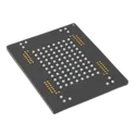
MT29F256G08AUCABH3-10ITZ:A
SLC NAND Flash Parallel/Serial 3.3V 256G-bit 32G x 8 100-Pin LBGA FLASH - NAND (SLC) Memory IC 256Gbit Parallel 100 MHz 100-LBGA (12x18) The MT29F256G08AUCABH3-10ITZ:A is a high-density 256Gb Single-Level Cell (SLC) NAND Flash memory device from Micron Technology. It provides non-volatile data storage with high reliability, fast read/write performance, and long endurance, making it suitable for industrial, networking, embedded computing, automotive, and data-logging applications. The device supports both asynchronous and synchronous interfaces and complies with the Open NAND Flash Interface (ONFI) standard for enhanced interoperability and performance. It is housed in a compact 100-ball LBGA package (12 mm × 18 mm). • Open NAND Flash Interface (ONFI) 2.2-compliant1 • Single-level cell (SLC) technology • Organization – Page size x8: 8640 bytes (8192 + 448 bytes) – Block size: 128 pages (1024K + 56K bytes) – Plane size: 2 planes x 2048 blocks per plane – Device size: 32Gb: 4096 blocks; 64Gb: 8192 blocks; 128Gb: 16,384 blocks; 256Gb: 32,768 blocks • Synchronous I/O performance – Up to synchronous timing mode 5 – Clock rate: 10ns (DDR) – Read/write throughput per pin: 200 MT/s • Asynchronous I/O performance – Up to asynchronous timing mode 5 – tRC/tWC: 20ns (MIN) – Read/write throughput per pin: 50 MT/s • Array performance – Read page: 35µs (MAX) – Program page: 350µs (TYP) – Erase block: 1.5ms (TYP) • Operating Voltage Range – VCC: 2.7–3.6V – VCCQ: 1.7–1.95V, 2.7–3.6V • Command set: ONFI NAND Flash Protocol • Advanced Command Set – Program cache – Read cache sequential – Read cache random – One-time programmable (OTP) mode – Multi-plane commands – Multi-LUN operations – Read unique ID – Copyback • First block (block address 00h) is valid when shipped from factory. For minimum required ECC, see Error Management (page 114). • RESET (FFh) required as first command after power-on • Operation status byte provides software method for detecting – Operation completion – Pass/fail condition – Write-protect status • Data strobe (DQS) signals provide a hardware method for synchronizing data DQ in the synchronous interface • Copyback operations supported within the plane from which data is read • Quality and reliability – Data retention: JESD47G compliant; see qualification report – Endurance: 60,000 PROGRAM/ERASE cycles • Operating temperature: – Commercial: 0°C to +70°C – Industrial (IT): –40ºC to +85ºC • Package – 52-pad LGA – 48-pin TSOP – 100-ball BGA – 132-ball BGA #Micron #NANDFlash #SLCNAND #FlashMemory #NonVolatileMemory #ONFI #EmbeddedSystems #IndustrialElectronics #DataStorage #MemoryIC #LBGA100 #HighReliability #MT29F256G08AUCABH310ITZA #MicronMemory #ParallelNANDFlash
1 Use
0 Stars