Capacitors
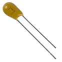
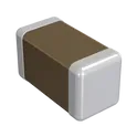
A capacitor is a passive electronic component that stores electrical charge and is commonly used to store energy in a circuit. Capacitors are used in a wide range of applications including power supply filtering, signal coupling, and decoupling, noise suppression, and voltage dividing. One of the main use cases of capacitors is to smooth out fluctuations in a direct current (DC) power supply by acting as a temporary reservoir of electrical charge. Capacitors can also be used to block the flow of direct current while allowing alternating current to pass, making them useful for signal coupling and decoupling in audio and radio frequency circuits. Flux.ai is the world's largest community-driven public library of capacitors, offering footprints, symbols, datasheets, and simulation models for a wide range of capacitor types. Whether you're an engineer looking for detailed technical information or a maker in need of resources for your latest project, Flux.ai has you covered.
ADXL335BCPZ
Accelerometer X, Y, Z Axis ±3g 1.6kHz (X,Y), 550Hz (Z) 16-LFCSP-LQ (4x4) The ADXL335BCPZ is a small, thin, low-power, complete 3-axis accelerometer with signal-conditioned voltage outputs. It measures acceleration with a minimum full-scale range of ±3 g. The device outputs analog voltages proportional to acceleration in each of the three orthogonal axes (X, Y, and Z). The accelerometer is designed for low power consumption and high resolution, making it suitable for mobile devices, tilt sensing, motion detection, and vibration monitoring. It operates over a wide temperature range and requires minimal external components, enabling easy integration into compact systems. Functional Overview The ADXL335 uses a capacitive sensing structure to detect acceleration. Changes in acceleration result in differential capacitance changes, which are converted into voltage outputs through an internal signal conditioning circuit. Each axis provides an independent analog output that can be directly interfaced with ADC inputs of microcontrollers or other processing units. Bandwidth for each axis can be adjusted using external capacitors, allowing flexibility depending on application requirements. Electrical Characteristics Supply Voltage Range: 1.8 V to 3.6 V Supply Current: Typical: 350 µA Measurement Range: ±3 g Sensitivity (Typical): 300 mV/g Zero-g Bias Level: Approximately mid-supply voltage Bandwidth: User-selectable via external capacitors Typical range: X, Y axes: up to 1600 Hz Z axis: up to 550 Hz Output Characteristics Output Type: Analog voltage (ratiometric to supply voltage) Number of Axes: Three (X, Y, Z) Output Noise: Low noise suitable for precision motion sensing Cross-Axis Sensitivity: Typically ±1% Mechanical Characteristics Package Type: 16-lead LFCSP (Lead Frame Chip Scale Package) Dimensions: Approximately 4 mm × 4 mm × 1.45 mm Mounting: Surface mount Environmental Specifications Operating Temperature Range: −40°C to +85°C Shock Survivability: Up to 10,000 g Interface Requirements External Components: Requires capacitors for bandwidth setting (one per axis) Output Interface: Direct analog output compatible with ADC inputs Applications Mobile devices and handheld electronics Tilt and orientation sensing Vibration monitoring systems Gaming and motion input devices Industrial instrumentation Wearable electronics Key Features Low power consumption Compact form factor High resolution analog outputs User-adjustable bandwidth Wide operating temperature range Simple integration with minimal external components #commonpartslibrary #sensor #transducer #motionsensor #accelerometer
58 Uses1 Stars
NE555P
The NE555 devices are precision timing circuits capable of producing accurate time delays or oscillation. In time-delay or monostable operating modes, the timed interval is controlled by a single external resistor and capacitor network. In the astable mode of operation, the frequency and duty cycle are controlled independently with two external resistors and a single external capacitor. Each timer has a trigger level equal to approximately one-third of the supply voltage and a threshold level equal to approximately two-thirds of the supply voltage. These levels can be altered by use of the control voltage pin (CONT). When the trigger input (TRIG) is less than the trigger level, the flip-flop is set and the output goes high. If TRIG is greater than the trigger level and the threshold input (THRES) is greater than the threshold level, the flip-flop is reset and the output is low. The reset input (RESET) overrides all other inputs and is used to initiate a new timing cycle. If RESET is low, the flip-flop is reset and the output is low. Whenever the output is low, a lowimpedance path is provided between the discharge pin (DISCH) and the ground pin (GND). Tie all unused inputs to an appropriate logic level to prevent false triggering. The output circuit is capable of sinking or sourcing current up to 200mA. Operation is specified for supplies of 5V to 15V. With a 5V supply, output levels are compatible with TTL inputs. Features - Timing from microseconds to hours - Astable or monostable operation - Adjustable duty cycle - TTL-compatible output can sink or source up to 200mA - On products compliant to MIL-PRF-38535, all parameters are tested unless otherwise noted. Applications - Pulse-shaping circuits - Missing-pulse detectors - Pulse-width modulators - Pulse-position modulators - Sequential timers - Pulse generators -F requency dividers - Industrial controls
2.4k Uses1 Stars