Timers and RTCs
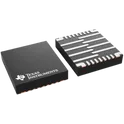
MAX77962EWJ12+T
Charger IC Lithium Ion 49-WLP (3.46x3.46) The MAX77962 is a high-performance wide-input 3.2A buck-boost charger with a Smart Power Selector™ and operates as a reverse buck without an additional inductor, allowing the IC to power USB On-the-Go (OTG) accessories. The device integrates low-loss power switches, and provides small solution size, high efficiency, low heat, and fast battery charging. The reverse buck has true-load disconnect and is protected by an adjustable output current limit. The device is highly flexible and programmable through I2C configuration or autonomously through resistor configuration. The battery charger includes a Smart Power Selector to accommodate a wide range of battery sizes and system loads. The Smart Power Selector allows the system to start up gracefully when an input source is available even when the battery is deeply discharged (dead battery) or missing. For battery safety/authentication reasons, the IC can be configured to keep charging disabled, and allow the DC-DC to switch and regulate the SYS voltage. The system processor can later enable charging using the appropriate I2C commands. Alternatively, the IC can be configured to automatically start charging. ● 3.5V to 23V Input Operating Range, 30VDC Withstand Voltage ● 97% Peak Efficiency at 9VIN/7.4VOUT/1.5AOUT ● Reverse Leakage Protection ● 50mA to 3.15A Programmable Input Current Limit ● 50mA to 3.2A Programmable Constant Current Charge ● Remote Differential Voltage Sensing ● 600kHz or 1.2MHz Switching Frequency Options ● System Instant On with Smart Power Selector PowerPath ● Charge Safety Timer ● Die Temperature Regulation with Thermal Foldback Loop ● Input Power Management with Adaptive Input Current Limit (AICL) and Input Voltage Regulation ● 10mΩ BATT to SYS Switch, Up to 10A Overcurrent Threshold ● Reverse Buck Mode 5.1V/1.5A to Support USB OTG ● JEITA Compliant with NTC Thermistor Monitor ● I 2C or Resistor Programmable ● 3.458mm x 3.458mm 49-Bump WLP #CommonPartsLibrary #IntegratedCircuit #PowerManagement #MAX77962
0 Uses
0 Stars
TPS259850RQPR
Electronic Fuse Regulator High-Side 60A 26-VQFN-HR (5x4.5) The TPS259850RQPR is an integrated eFuse power protection device designed for robust power path management in low-voltage DC systems. Manufactured by Texas Instruments, this device provides advanced protection features including overvoltage protection, undervoltage protection, overcurrent limiting, short-circuit protection, reverse current blocking, and thermal shutdown. The device is optimized for applications requiring controlled inrush current, fault isolation, and system reliability in industrial, automotive, telecommunications, and embedded electronic systems. The TPS259850RQPR supports a wide operating input voltage range and integrates programmable protection thresholds to allow flexible system-level configuration. The device includes an internal MOSFET with low on-resistance for efficient power delivery while minimizing power dissipation. Fast fault response and automatic retry functionality enhance system robustness and reduce the need for external supervisory circuitry. The device is housed in a compact QFN package suitable for space-constrained PCB designs and supports high-current operation with efficient thermal performance. The integrated protection architecture simplifies power subsystem design while improving reliability and fault tolerance. Electrical Characteristics Input operating voltage range supports low-voltage DC power rails commonly used in embedded and industrial systems. Integrated low-RDS(on) MOSFET minimizes conduction losses and improves overall efficiency. Programmable current limiting enables configurable overcurrent protection. Fast short-circuit response protects downstream circuitry during fault events. Adjustable overvoltage and undervoltage thresholds allow flexible supply monitoring. Reverse current blocking prevents back-drive conditions and protects power sources. Thermal shutdown protection disables the device during excessive junction temperature conditions. Controlled output slew rate limits inrush current during startup and hot-plug events. Automatic retry and latch-off fault management modes are supported. Power-good indication output provides system power status monitoring. Protection Features Overcurrent protection with programmable current limit threshold. Short-circuit protection with rapid fault response. Input overvoltage protection. Input undervoltage lockout protection. Reverse current and reverse polarity protection support. Thermal shutdown with automatic recovery capability. Fault timer control for transient fault management. Safe hot-swap and hot-plug operation support. Mechanical Characteristics Package type is QFN with compact footprint optimized for high-density PCB layouts. Surface-mount device compatible with automated assembly processes. Thermally enhanced package construction improves heat dissipation. RoHS-compliant and suitable for lead-free manufacturing processes. Applications Industrial power distribution systems. Automotive electronic subsystems. Telecommunication and networking equipment. Server and storage platforms. Hot-swappable modules. USB Type-C and power delivery systems. Embedded computing platforms. FPGA and processor power rail protection. Battery-powered and portable electronic equipment. #commonpartslibrary #integratedcircuit #powermanagement #regulator
6 Uses
0 Stars
TPS6593C3A0RWERQ1
Power Management Specialized - PMIC Automotive 2.8-V to 5.5-V PMIC The TPS6593C3A0RWERQ1 is an automotive-grade power management integrated circuit (PMIC) designed by Texas Instruments for advanced processor and system-on-chip power architectures. The device integrates multiple high-efficiency DC/DC buck converters, low-dropout regulators, power sequencing, safety monitoring, and diagnostic functions into a single compact package. It is optimized for use in automotive ADAS, digital cockpit, gateway, radar, vision, and domain controller applications requiring functional safety compliance and high power density. The device supports complex multi-rail power management for high-performance processors and includes configurable startup and shutdown sequencing, voltage monitoring, watchdog functionality, error signaling, and fault protection mechanisms. Integrated communication interfaces enable configuration and monitoring by an external host processor. The PMIC is qualified for automotive applications and supports operation across extended temperature ranges suitable for harsh automotive environments. Key Features Automotive AEC-Q100 qualified power management IC for processor power systems Integrated multi-phase step-down buck converters for high-current rails Integrated low-dropout linear regulators for analog and auxiliary rails Programmable power sequencing and rail management Functional safety support suitable for ASIL-oriented system architectures Integrated watchdog timer and safety monitoring functions Voltage supervision and fault detection for all major rails I2C and SPI communication interface support Power-good outputs and interrupt signaling Thermal shutdown and overtemperature protection Overcurrent and short-circuit protection Undervoltage and overvoltage monitoring Configurable GPIO functionality Low-power standby and sleep mode support Optimized for automotive SoCs and processors High-efficiency switching regulator architecture Compact VQFN package with thermal enhancement Electrical Characteristics Input supply voltage range supports automotive battery-powered systems Multiple programmable buck converter output voltages Integrated LDO outputs for precision analog and digital domains High switching frequency operation for reduced external component size Wide operating junction temperature range suitable for automotive environments Low shutdown current for standby operation High-current capability for processor core supplies Accurate voltage regulation and monitoring Protection and Safety Features Thermal shutdown protection Buck converter cycle-by-cycle current limiting Short-circuit protection on power rails Undervoltage lockout protection Power sequencing fault management Watchdog monitoring for processor supervision Diagnostic interrupt and fault reporting capability Safe-state transition support during fault conditions Package Information Package type: VQFN Package option: RWE Automotive-grade Q1 qualified device RoHS compliant Surface-mount package optimized for thermal performance Typical Applications Automotive domain controllers ADAS processing modules Digital cockpit systems Automotive gateway and networking platforms Radar and vision systems Processor and FPGA power management Industrial high-performance embedded systems #commonpartslibrary #integratedcircuit #powermanagement
1 Use
0 Stars
BQ25792RQMR
Charger IC Lithium Ion/Polymer 29-VQFN-HR (4x4) The BQ25792 is a switch-mode synchronous buck-boost charger with full power-path management. It can automatically regulate power flow between the input source, system load, and battery. It supports a wide input range and is designed for USB Type-C™ / USB Power Delivery (USB-PD) systems, enabling both charging and OTG (power output from battery) operation. ⭐ Key Features ⚡ High-performance charging Up to 5 A charge current Supports 1S to 4S battery packs High efficiency (up to ~96% under typical conditions) Programmable switching frequency: 750 kHz or 1.5 MHz 🔋 Wide input support Input voltage range: 3.6 V to 24 V Absolute max rating up to 30 V Supports USB adapters and barrel jack sources Detects USB charging standards (BC1.2, DCP, CDP, HVDCP, etc.) 🔄 Buck-boost power conversion Seamless buck, boost, and buck-boost operation Maintains stable system voltage even when battery is low or input varies 🔌 USB-PD / OTG support USB Power Delivery (PD 3.0 compatible) Supports OTG output (battery powers USB port) OTG voltage range: 2.8 V to 22 V 🧠 Intelligent power management NVDC power path management (system can run without battery) Dual-input power mux controller (select between two power sources) Battery supplement mode (prevents input overload) 📊 Monitoring & control Integrated 16-bit ADC for voltage, current, temperature monitoring Fully I²C configurable Autonomous or host-controlled operation 🛡️ Protection & safety Input and battery over-voltage/over-current protection Thermal regulation and shutdown Charging safety timer MOSFET protection (internal switching FETs included) 📦 Package 29-pin VQFN (4 mm × 4 mm) package Industrial temperature range: -40°C to 85°C #CommonPartsLibrary #IntegratedCircuit #PowerManagement #Battery-charger
9 Uses
0 Stars
TLC555IDR
555 Type, Timer/Oscillator (Single) IC 2.1MHz 8-SOIC The TLC555IDR is a low-power CMOS timer device designed as a functional replacement for the standard bipolar 555 timer while providing significantly reduced supply current and improved operating efficiency. The device supports both astable and monostable operating modes and is commonly used for timing generation, pulse shaping, oscillation, PWM generation, delay circuits, and frequency generation applications. The CMOS architecture enables low power consumption, rail-to-rail output capability, and stable timing performance over a wide operating voltage range. The device is suitable for battery-powered systems, portable electronics, industrial controls, instrumentation, consumer products, and embedded electronic designs. The TLC555IDR is supplied in a compact SOIC surface-mount package intended for automated PCB assembly and space-constrained applications. Electrical Characteristics CMOS low-power timer architecture Functional equivalent to standard 555 timer devices Wide operating supply voltage range Low quiescent supply current High input impedance Rail-to-rail output swing capability Stable threshold and trigger levels Compatible with TTL and CMOS logic levels Capable of astable and monostable operation Adjustable duty cycle and frequency operation High output drive capability for direct interfacing Low noise and improved switching performance compared to bipolar 555 timers Functional Features Precision timing generation Oscillator and clock generation Pulse-width modulation support One-shot pulse generation Delay timer implementation Missing pulse detection Frequency divider implementation Sequential timing control LED flashing and tone generation PWM motor and power control applications Package Information Surface-mount SOIC package Standard tape-and-reel packaging format Compact footprint for automated assembly RoHS compliant device construction Environmental and Operating Conditions Industrial operating temperature range ESD protection handling required Suitable for commercial and industrial embedded systems Designed for low-power electronic applications Typical Applications Timer circuits Pulse generators Oscillators PWM controllers LED flashers Alarm and tone generators Frequency generators Power management timing Embedded control systems Portable battery-powered electronics #commonpartslibrary #integratedcircuit #timer #oscillator
39 Uses
0 Stars
TPS259814ARPWR
Electronic Fuse Regulator High-Side 10A 10-VQFN-HR (2x2) The TPS25981xx family of eFuses is a highly integrated circuit protection and power management solution in a small package. The devices provide multiple protection modes using very few external components and are a robust defense against overloads, short circuits, voltage surges and excessive inrush current. Output slew rate and inrush current can be adjusted using a single external capacitor. Loads are protected from input overvoltage conditions by cutting off the output if input exceeds an adjustable overvoltage threshold. The devices respond to output overload by actively limiting the current (during startup) or breaking the circuit (during steady-state). The overcurrent protection threshold as well as the transient overcurrent blanking timer are useradjustable. The current limit control pin also functions as an analog load current monitor. The devices are available in a 2-mm × 2-mm, 10- pin HotRod™ QFN package for improved thermal performance and reduced system footprint. The devices are characterized for operation over a junction temperature range of –40°C to +125°C. • Wide operating input voltage range: 2.7 V to 16 V – 20-V absolute maximum • Integrated FET with low on-resistance: RON = 6 mΩ (typ.) • Fast overvoltage protection – Adjustable overvoltage lockout (OVLO) with 1.2-μs (typ.) response time • Overcurrent protection with load current monitor output (ILM) – Circuit-breaker response – Adjustable threshold (ILIM) 1.5 A – 11 A • ±10% accuracy for ILIM > 5 A – Adjustable transient blanking timer (ITIMER) to allow peak currents up to 2 × ILIM – Output load current monitor accuracy: ±10% (IOUT ≥ 3 A) • Fast-trip response for short-circuit protection – 640-ns (typ.) response time – Adjustable (2 × ILIM) and fixed thresholds • Active high enable input with adjustable undervoltage lockout threshold (UVLO) • Active low enable input with adjustable undervoltage lockout threshold (OVLO) • Adjustable output slew rate control (dVdt) • Option to drive external FET for reverse current blocking in disabled/OFF state • Overtemperature protection • Quick Output Discharge • Digital outputs – Power Good (PG) and fault indication (FLT) • UL 2367 recognition (pending) • IEC 62368 CB certification (pending) • Small footprint: QFN 2-mm × 2-mm, 0.45-mm pitch #CommonPartsLibrary #IntegratedCircuit #PowerManagement
17 Uses
0 Stars
dsPIC33CK256MP205-I/M4
dsPIC dsPIC™ 33CK, Functional Safety (FuSa) Microcontroller IC 16-Bit 100MHz 256KB (256K x 8) FLASH 48-UQFN (6x6) 28/36/48/64/80-Pin Digital Signal Controllers with High-Resolution PWM and CAN Flexible Data (CAN FD) Operating Conditions • 3.0V to 3.6V, -40°C to +125°C, DC to 100 MIPS • 3.0V to 3.6V, -40°C to +150°C, DC to 70 MIPS Core: 16-Bit dsPIC33CK CPU • 32-256 Kbytes of Program Flash with ECC and 8-24K RAM • Fast 6-Cycle Divide • LiveUpdate • Code Efficient (C and Assembly) Architecture • 40-Bit Wide Accumulators • Single-Cycle (MAC/MPY) with Dual Data Fetch • Single-Cycle, Mixed-Sign MUL Plus Hardware Divide • 32-Bit Multiply Support • Four Sets of Interrupt Context Saving Registers which Include Accumulator and STATUS for Fast Interrupt Handling • Zero Overhead Looping • RAM Memory Built-In Self-Test (MBIST) Clock Management • Internal Oscillator • Programmable PLLs and Oscillator Clock Sources • Reference Clock Output • Fail-Safe Clock Monitor (FSCM) • Fast Wake-up and Start-up • Backup Internal Oscillator Power Management • Low-Power Management Modes (Sleep, Idle, Doze) • Integrated Power-on Reset and Brown-out Reset High-Speed PWM • Eight PWM Pairs • Up to 250 ps PWM Resolution • Dead Time for Rising and Falling Edges • Dead-Time Compensation • Clock Chopping for High-Frequency Operation • PWM Support for: - DC/DC, AC/DC, inverters, PFC, lighting - BLDC, PMSM, ACIM, SRM motors • Fault and Current Limit Inputs • Flexible Trigger Configuration for ADC Triggering Timers/Output Compare/Input Capture • One General Purpose Timer • Peripheral Trigger Generator (PTG): - Up to 15 trigger sources to other peripheral modules - CPU independent state machine-based instruction sequencer • Nine MCCP/SCCP modules which Include Timer, Capture/Compare and PWM: - One MCCP - Eight SCCPs - 16 or 32-bit time base - 16 or 32-bit capture - 4-deep capture buffer • Fully Asynchronous Operation, Available in Sleep Modes #CommonPartsLibrary #IntegratedCircuit #Microcontroller #DSPIC33CK256MP
4 Uses
0 Stars
STM32F103C8T6
ARM® Cortex® M3 STM32F1 Microcontroller IC 32-Bit Single-Core 72MHz 64KB (64K x 8) FLASH Medium-density performance line Arm®-based 32-bit MCU with 64 or 128 KB Flash, USB, CAN, 7 timers, 2 ADCs, 9 com. interfaces Arm® 32-bit Cortex®-M3 CPU core – 72 MHz maximum frequency, 1.25 DMIPS/MHz (Dhrystone 2.1) performance at 0 wait state memory access – Single-cycle multiplication and hardware division • Memories – 64 or 128 Kbytes of Flash memory – 20 Kbytes of SRAM • Clock, reset and supply management – 2.0 to 3.6 V application supply and I/Os – POR, PDR, and programmable voltage detector (PVD) – 4 to 16 MHz crystal oscillator – Internal 8 MHz factory-trimmed RC – Internal 40 kHz RC – PLL for CPU clock – 32 kHz oscillator for RTC with calibration • Low-power – Sleep, Stop and Standby modes – VBAT supply for RTC and backup registers • 2x 12-bit, 1 µs A/D converters (up to 16 channels) – Conversion range: 0 to 3.6 V – Dual-sample and hold capability – Temperature sensor • DMA – 7-channel DMA controller – Peripherals supported: timers, ADC, SPIs, I 2Cs and USARTs • Up to 80 fast I/O ports – 26/37/51/80 I/Os, all mappable on 16 external interrupt vectors and almost all 5 V-tolerant Debug mode: – Serial wire debug (SWD) and JTAG interfaces • Seven timers – Three 16-bit timers, each with up to 4 IC/OC/PWM or pulse counter and quadrature (incremental) encoder input – 16-bit, motor control PWM timer with dead-time generation and emergency stop – Two watchdog timers (independent and window) – SysTick timer 24-bit downcounter • Up to nine communication interfaces – Up to two I2C interfaces (SMBus/PMBus®) – Up to three USARTs (ISO 7816 interface, LIN, IrDA capability, modem control) – Up to two SPIs (18 Mbit/s) – CAN interface (2.0B Active) – USB 2.0 full-speed interface • CRC calculation unit, 96-bit unique ID • Packages are ECOPACK #commonpartslibrary #integratedcircuit #microcontroller #stm32f1
26 Uses
0 Stars
PIC32MZ2048EFM100-I/PT
MIPS32® M-Class PIC® 32MZ Microcontroller IC 32-Bit 200MHz 2MB (2M x 8) FLASH 100-TQFP (12x12) The PIC32MZ2048EFM100-I/PT is built around a MIPS32® M-Class core operating at up to 200 MHz, delivering high computational performance suitable for real-time control, signal processing, and communication-intensive systems. It integrates large on-chip memory, multiple communication interfaces, and rich peripheral support in a compact package. Key Features Core Architecture: 32-bit MIPS32® M-Class CPU Clock Speed: Up to 200 MHz Program Memory: 2 MB Flash RAM: 512 KB Package: 100-pin TQFP (12×12 mm), surface-mount Operating Voltage: 2.1 V to 3.6 V I/O Pins: Up to 78 programmable I/O Integrated Peripherals & Interfaces Communication Interfaces: CAN, Ethernet, USB OTG I²C, SPI, SQI, UART/USART Parallel Master Port (PMP) Analog Features: 40-channel, 12-bit ADC System Peripherals: DMA controller PWM modules Watchdog timer (WDT) Brown-out reset and power-on reset Advanced Features: Floating Point Unit (FPU) for fast math operations Hardware crypto engine (AES, SHA, etc., depending on variant) High-speed USB and Ethernet connectivity #CommonPartsLibrary #IntegratedCircuit #Microcontroller #PIC® 32MZ
2 Uses
0 Stars