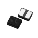
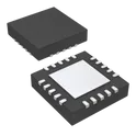
Oscillators
An oscillator is an electronic circuit that generates a periodic, oscillating signal, often a sine wave or a square wave. Oscillators are used in a wide range of applications, including clocks, radios, and sound synthesis. Flux.ai has the world's largest community-driven public library of oscillators, with footprints, symbols, datasheets, and simulation models. This comprehensive resource allows engineers and designers to easily find the oscillator they need for their specific application and use it with confidence. Whether you are working on a simple clock circuit or a complex radio transmitter, Flux.ai's oscillator library has you covered. So, if you are in need of an oscillator for your next project, be sure to check out Flux.ai's extensive collection.
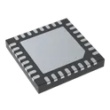
LAN8770M-I/PRA
4/4 Transceiver Full MII, RMII 32-VQFN (5x5) ## Engineering Specification ## General Description The **LAN8770M-I/PRA** is a Microchip Technology single-port **100BASE-T1 Ethernet physical layer transceiver** designed for automotive, industrial, and embedded networking applications. It provides Ethernet communication over a single balanced twisted pair and is suitable for compact systems requiring reliable network connectivity, low-power operation, and standard MAC interface support. The device is commonly used in automotive electronic control units, infotainment systems, telematics modules, sensor nodes, industrial control systems, and embedded Ethernet hardware. ## Device Identification Manufacturer Part Number: **LAN8770M-I/PRA** Manufacturer: **Microchip Technology** Product Family: **LAN8770** Device Category: **Integrated Circuit** Device Type: **Ethernet PHY Transceiver** Ethernet Standard: **100BASE-T1** Interface Type: **MII and RMII** Mounting Type: **Surface Mount** Package Type: **VQFN** ## Functional Description The device functions as an Ethernet physical layer transceiver that connects a host controller or microcontroller MAC interface to a single-pair Ethernet physical medium. It handles the analog and digital PHY functions required for 100BASE-T1 communication, allowing embedded systems to transmit and receive Ethernet data over a single twisted pair cable. ## Network and Interface Description The **LAN8770M-I/PRA** supports 100 Mb/s single-pair Ethernet communication and provides MII and RMII host interface options. This allows integration with microcontrollers, processors, gateways, and network controllers that support standard Ethernet MAC interfaces. The device is intended for applications where compact Ethernet connectivity and reduced cabling complexity are required. ## Electrical Description The device is designed for low-voltage operation and supports multiple supply domains according to the manufacturer’s recommended operating conditions. Proper power sequencing, decoupling, reset handling, clocking, and reference layout should be implemented to maintain stable PHY operation and signal integrity. ## Package and Mechanical Description The component is supplied in a compact surface-mount **VQFN package**, suitable for dense printed circuit board assemblies. The package supports automated assembly and is appropriate for space-constrained automotive and industrial electronic designs. ## Control and Diagnostic Description The PHY supports management and configuration through standard control interfaces used in Ethernet designs. It provides status monitoring and configuration capability for link management, operating mode selection, and system-level diagnostics. These features allow the host controller to configure and monitor Ethernet link behavior during operation. ## Automotive and Industrial Suitability The **LAN8770M-I/PRA** is suitable for embedded systems requiring robust single-pair Ethernet communication. It is applicable to automotive networking, telematics, infotainment, advanced driver assistance systems, industrial Ethernet nodes, building automation, control modules, and other connected embedded platforms. ## Mounting and Assembly Description The component is intended for surface-mount PCB assembly using standard reflow soldering processes. PCB layout should follow Microchip’s hardware design guidance, including proper power supply decoupling, controlled impedance routing, short signal paths, grounding, and separation of sensitive analog and digital sections where applicable. ## Design Considerations The design should account for Ethernet signal integrity, single-pair cable interface requirements, common-mode noise control, EMC performance, supply filtering, oscillator or clock source requirements, reset timing, thermal performance, and package solderability. The device should not be operated beyond the manufacturer’s specified electrical, thermal, or mechanical limits. ## Application Suitability The device is suitable for automotive Ethernet nodes, electronic control units, telematics modules, infotainment systems, sensor interfaces, industrial controllers, embedded gateways, connected equipment, and compact network-enabled hardware requiring 100BASE-T1 Ethernet PHY functionality. ## Hashtags #commonpartslibrary #integratedcircuit #ethernetphy #microchip #microchiptechnology #lan8770 #lan8770mipra #singlepairethernet #100baset1 #automotiveethernet #ethernettransceiver #phytransceiver #embeddednetworking #mii #rmii #vqfnpackage #smdcomponent #surfacemount #automotiveelectronics #industrialethernet #telematics #infotainment #embeddedhardware #pcbdesign #hardwaredesign #electronicscomponents #electronicparts #componentlibrary #engineeringparts #electronicsengineering
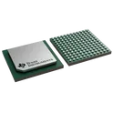
2 Uses0 StarsADC09SJ1300AAVT
Analog to Digital Converters - ADC Single-channel, 9-bit, 1.3-GSPS analog-to-digital converter (ADC) with JESD204C interface 144-FCBGA -40 to 85 ADC09xJ1300 is a family of quad, dual and single channel, 9-bit, 1.3GSPS analog-to-digital converters (ADC). Low power consumption, high sampling rate and 9-bit resolution makes the ADC09xJ1300 ideally suited for suited for a variety of multi-channel communications and test systems. Full-power input bandwidth (-3dB) of 6GHz enables direct RF sampling of L-band and S-band. A number of clocking features are included to relax system hardware requirements, such as an internal phase-locked loop (PLL) with integrated voltagecontrolled oscillator (VCO) to generate the sampling clock. Four clock outputs are provided to clock the logic and SerDes of the FPGA or ASIC. A timestamp input and output is provided for pulsed systems. JESD204C serialized interface decreases system size by reducing the amount of printed circuit board (PCB) routing. Interface modes support from 2 to 8 lanes (dual and quad channel devices) or 1 to 4 lanes (for the single channel device), with SerDes baud-rates up to 17.16Gbps, to allow the optimal configuration for each application. Features • ADC Core: – Resolution: 9 Bit – Maximum sampling rate: 1.3GSPS – Non-interleaved architecture – Internal dither reduces high-order harmonics • Performance specifications (–1dBFS): – SNR (100 MHz): 53.5dBFS – ENOB (100 MHz): 8.5 Bits – SFDR (100 MHz): 64dBc – Noise floor (–20dBFS): –143dBFS • Full-scale input voltage: 80 mVPP-DIFF • Full-power input bandwidth: 6GHz • JESD204C Serial data interface: – Support for 2 to 8 (Quad/Dual channel) or 1 to 4 (Single channel) total SerDes lanes – Maximum baud-rate: 17.16Gbps – 64B/66B and 8B/10B encoding modes – Subclass-1 support for deterministic latency – Compatible with JESD204B receivers • Optional internal sampling clock generation – Internal PLL and VCO (7.2–8.2GHz) • SYSREF Windowing eases synchronization • Four clock outputs simplify system clocking – Reference clocks for FPGA or adjacent ADC – Reference clock for SerDes transceivers • Timestamp input and output for pulsed systems • Power consumption (1GSPS): – Quad Channel: 450mW / channel – Dual channel: 625mW / channel – Single channel: 940mW • Power supplies: 1.1V, 1.9V #CommonPartsLibrary #IntegratedCircuit #ADC #HighSpeedADC #RFADC #JESD204C #13GSPS #9bitADC #DirectRFSampling #TexasInstruments #MixedSignal #DataAcquisition #JESD204
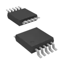
0 Uses0 StarsINA228AIDGSR
Power Supply Controller Digital Power Monitor 10-VSSOP The INA228 is an ultra-precise digital power monitor with a 20-bit delta-sigma ADC specifically designed for current-sensing applications. The device can measure a full-scale differential input of ±163.84 mV or ±40.96 mV across a resistive shunt sense element with common-mode voltage support from –0.3 V to +85 V. The INA228 reports current, bus voltage, temperature, power, energy and charge accumulation while employing a precision ±0.5% integrated oscillator, all while performing the needed calculations in the background. The integrated temperature sensor is ±1°C accurate for die temperature measurement and is useful in monitoring the system ambient temperature. The low offset and gain drift design of the INA228 allows the device to be used in precise systems that do not undergo multi-temperature calibration during manufacturing. Further, the very low offset voltage and noise allow for use in mA to kA sensing applications and provide a wide dynamic range without significant power dissipation losses on the sensing shunt element. The low input bias current of the device permits the use of larger currentsense resistors, thus providing accurate current measurements in the micro-amp range. The device allows for selectable ADC conversion times from 50 µs to 4.12 ms as well as sample averaging from 1x to 1024x, which further helps reduce the noise of the measured data. • High-resolution, 20-bit delta-sigma ADC • Current monitoring accuracy: – Offset voltage: ±1 µV (maximum) – Offset drift: ±0.01 µV/°C (maximum) – Gain error: ±0.05% (maximum) – Gain error drift: ±20 ppm/°C (maximum) – Common mode rejection: 154 dB (minimum) • Power monitoring accuracy: – 0.5% full scale, –40°C to +125°C (maximum) • Energy and charge accuracy: – 1.0% full scale (maximum) • Fast alert response: 75 μs • Wide common-mode range: –0.3 V to +85 V • Bus voltage sense input: 0 V to 85 V • Shunt full-scale differential range: ±163.84 mV / ±40.96 mV • Input bias current: 2.5 nA (maximum) • Temperature sensor: ±1°C (maximum at 25°C) • Programmable resistor temperature compensation • Programmable conversion time and averaging • 2.94-MHz high-speed I2C interface with 16 pinselectable addresses • Operates from a 2.7-V to 5.5-V supply: – Operational current: 640 µA (typical) – Shutdown current: 5 µA (maximum) #CommonPartsLibrary #IntegratedCircuit #PowerManagement
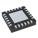
170 Uses0 StarsCP2102N-A02-GQFN24
USB-to-UART Bridge CP2102N-A02-GQFN24 is a highly integrated USB-to-UART bridge controller from Silicon Labs. It provides a simple and cost-effective way to add USB connectivity to embedded systems by converting USB 2.0 Full-Speed communication into a standard UART interface. The device integrates the USB transceiver, oscillator, voltage regulator, and UART controller, minimizing external components and eliminating the need for USB firmware development. It is commonly used in microcontroller programming interfaces, industrial equipment, POS terminals, data loggers, and USB-to-serial adapters. Key Features USB 2.0 Full-Speed compliant (12 Mbps) interface. USB-to-UART bridge with data rates up to 3 Mbaud. Integrated USB transceiver; no external USB resistors required. Integrated oscillator; no external crystal required. On-chip 3.3 V voltage regulator. USB Battery Charger Detection (BC 1.2) support. Remote wakeup capability from USB suspend state. Low operating current of approximately 9.5 mA. Hardware and software flow control support. Internal configurable ROM for Vendor ID, Product ID, serial number, and USB descriptors. Royalty-free Virtual COM Port (VCP) drivers available for major operating systems. Operating temperature range: −40°C to +85°C. Compact 24-pin QFN (4 mm × 4 mm) package. Typical Applications USB-to-Serial adapters Microcontroller programming and debugging interfaces Industrial automation equipment Point-of-sale (POS) terminals Medical instruments Data acquisition and logging systems Embedded systems requiring USB connectivity #commonpartslibrary #integratedcircuit
219 Uses0 StarsNX3225GD 8.000MHZ STD-CRA-3
The NX3225GD 8.000MHz STD-CRA-3 is a surface-mount quartz crystal resonator designed to provide a stable and accurate clock reference for electronic circuits. It is housed in a compact ceramic package suitable for space-constrained applications and is optimized for low power consumption and reliable frequency generation. This crystal is commonly used in microcontrollers, wireless communication modules, industrial control systems, consumer electronics, IoT devices, and embedded systems requiring precise timing and frequency control. Features Fundamental mode quartz crystal resonator Nominal frequency of 8.000 MHz Compact surface-mount ceramic package High frequency stability and accuracy Low equivalent series resistance Suitable for low-power oscillator circuits Excellent aging characteristics RoHS-compliant construction Designed for automated SMT assembly processes Reliable operation across industrial temperature environments Electrical Characteristics Crystal type: Quartz Crystal Resonator Frequency: 8.000 MHz Oscillation mode: Fundamental Load capacitance: Standard load capacitance configuration Frequency tolerance: Standard precision grade Frequency stability: Industrial-grade stability performance Equivalent series resistance optimized for MCU and RF oscillator circuits Low drive level operation High insulation resistance Mechanical Characteristics Surface-mount package Ceramic hermetic enclosure Compact footprint suitable for high-density PCB layouts Compatible with standard reflow soldering processes Designed for automated pick-and-place assembly Applications Microcontroller clock generation Wireless communication devices Bluetooth and RF modules IoT and smart devices Industrial automation equipment Embedded control systems Consumer electronics Timing and synchronization circuits Sensor interface modules Portable battery-powered products Compliance RoHS compliant Lead-free package Environmentally friendly manufacturing standards Suitable for commercial and industrial electronic applications #commonpartslibrary #crystal #quartzcrystal #frequencycontrol #timingdevice #clocksource #oscillator #smtcomponent #embeddedsystems #wirelesscommunication #industrialelectronics #consumerelectronics #iotdevices #passivecomponents #electroniccomponents
31 Uses0 StarsCC1101RGP
The CC1101RGP is a low-power sub-gigahertz RF transceiver designed for wireless communication applications requiring reliable long-range data transmission and high receiver sensitivity. It integrates a complete radio frequency front-end, packet handling engine, modulation and demodulation circuitry, frequency synthesizer, and advanced power management features within a compact package. The device supports multiple modulation formats and is optimized for industrial, scientific, medical, smart metering, home automation, remote control, wireless sensor networks, and Internet of Things applications. Its flexible configuration options enable designers to achieve an optimal balance between communication range, data throughput, power consumption, and system robustness. Features Sub-gigahertz RF transceiver for license-free ISM frequency bands High receiver sensitivity for extended communication range Programmable output power for optimized power consumption Multiple modulation schemes including FSK, GFSK, ASK, OOK, and MSK Integrated packet handling and error detection functions Fast frequency synthesizer settling time Low current consumption in transmit, receive, and sleep modes Hardware support for address filtering and data buffering Programmable channel spacing and data rate configuration Integrated RSSI, LQI, and clear channel assessment functions SPI interface for configuration and data communication Suitable for battery-powered wireless devices Applications Smart metering systems Wireless sensor networks Industrial monitoring and control Home and building automation Remote keyless entry systems Alarm and security systems Asset tracking devices Telemetry and data acquisition systems IoT communication nodes Proprietary wireless communication networks Electrical Characteristics Wide operating supply voltage range Low-power transmit and receive operation Programmable RF output power levels High-performance frequency synthesizer Low standby and sleep current consumption Integrated crystal oscillator support Robust RF performance across supported frequency bands Interface and Connectivity Serial Peripheral Interface communication Digital control and status signals Configurable interrupt outputs Integrated FIFO buffers for transmit and receive data External antenna connection through matching network Package Information Surface-mount package suitable for automated assembly Compact footprint for space-constrained applications RoHS-compliant device construction #commonpartslibrary #integratedcircuit #wirelesscommunication #rftransceiver #subghz #iot #embeddedsystems #industrialautomation #smartmetering #wirelesssensornetwork #lowpowerdesign #telemetry #homeautomation #remotecontrol #texasinstruments
84 Uses0 Stars