Interface ICs
An interface IC is a type of integrated circuit that is designed to facilitate communication between two devices or systems. These devices are commonly used in electronic systems to enable the transfer of data and control signals between different components or subsystems. Some common use cases for interface ICs include connecting microcontrollers to peripherals such as sensors or displays, linking multiple processors together in a network, and enabling communication between devices using different communication protocols. Flux.ai has the world's largest community-driven public library of interface ICs, with footprints, symbols, datasheets, and simulation models. This library is a valuable resource for engineers and designers who need access to accurate and up-to-date information on these important components. Whether you are working on a new design project or simply looking to learn more about interface ICs, Flux.ai is an excellent resource to help you find the information you need.
QMC5883L
Magnetic Sensors QMC5883L LGA-16_L3.0-W3.0-P0.50-BL_SQ The QMC5883L is a multi-chip three-axis magnetic sensor. This surface -mount, small sized chip has integrated magnetic sensors with signal condition ASIC, targeted for high precision applications such as compassing, navigation and gaming in drone, robot, mobile and personal hand-held devices. The QMC5883L is based on our state-of-the-art, high resolution, magneto-resistive technology licensed from Honeywell AMR technology. Along with custom-designed 16-bit ADC ASIC, it offers the advantages of low noise, high accuracy, low power consumption, offset cancellation and temperature compensation. QMC5883L enables 1° to 2° compass heading accuracy. The I²C serial bus allows for easy interface. The QMC5883L is in a 3x3x0.9mm3 surface mount 16-pin land grid array (LGA) package. 3-Axis Magneto-Resistive Sensors in a 3x3x0.9 mm3 Land Grid Array Package (LGA), guaranteed to operate over an extended temperature range of -40 °C to +85 °C. Small Size for Highly Integrated Products. Signals Have Been Digitized And Calibrated. 16 Bit ADC With Low Noise AMR Sensors Achieves 2 Milli-Gauss Field Resolution Enables 1° To 2° Degree Compass Heading Accuracy , Allows for Navigation and LBS Applications Wide Magnetic Field Range (±8 Gauss) Maximizes Sensor’s Full Dynamic Range and Resolution Temperature Compensated Data Output and Temperature Output Automatically Maintains Sensor’s Sensitivity Under Wide Operating Temperature Range I 2C Interface with Standard and Fast Modes. High-Speed Interfaces for Fast Data Communications. Maximum 200Hz Data Output Rate Wide Range Operation Voltage (2.16V To 3.6V) and Low Power Consumption (75A) Compatible with Battery Powered Applications Lead Free Package Construction RoHS Compliance Software And Algorithm Support Available Compassing Heading, Hard Iron, Soft Iron, and Auto Calibration Libraries Available #CommonPartsLibrary #Sensor
62 Uses0 StarsSMBJ6.8CA
The SMBJ6.8CA is a bidirectional Transient Voltage Suppression (TVS) diode designed to protect sensitive electronic circuits from voltage transients caused by electrostatic discharge, lightning-induced surges, inductive load switching, and other transient events. It is commonly used in power supplies, communication interfaces, industrial control systems, automotive electronics, and consumer devices requiring robust overvoltage protection. The device utilizes avalanche breakdown technology to rapidly clamp transient voltages to safe levels, helping prevent damage to downstream components. Its bidirectional configuration makes it suitable for protecting AC lines and signal lines where voltage polarity may reverse. The SMB package provides a compact surface-mount solution with high surge-handling capability and excellent reliability for demanding environments. Features Bidirectional transient voltage suppression diode Fast response time to transient events High peak pulse power dissipation capability Low incremental surge resistance Excellent clamping performance Surface-mount SMB package Protection against ESD and lightning-induced surges Suitable for AC and bidirectional signal line protection RoHS-compliant and halogen-free options available from various manufacturers High reliability and long operational life Electrical Characteristics Reverse standoff voltage optimized for low-voltage applications Avalanche breakdown protection mechanism High peak surge current capability Low leakage current during normal operation Bidirectional voltage clamping characteristics Designed for transient suppression in accordance with industry surge standards Applications Power input protection Communication interfaces Industrial automation equipment Automotive electronic modules Consumer electronics Data and signal line protection Telecom equipment Embedded control systems Sensor interface protection Package Information Package Type: SMB (DO-214AA) Surface-mount technology Compact footprint for PCB integration Suitable for automated assembly processes #commonpartslibrary #semiconductor #tvsdiode #esdprotection #surgeprotection #circuitprotection #transientvoltagesuppressor #powerprotection #electronics #surfaceMountDevice #automotiveelectronics #industrialelectronics
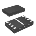
104 Uses0 StarsW25Q16JVUXIQ
SPI Flash Serial Flash Memory with Dual/Quad SPI The W25Q16JVUXIQ is a 16-Mbit (2-MByte) Serial NOR Flash memory device from Winbond. It is designed for embedded systems that require non-volatile code and data storage with minimal pin count, low power consumption, and high-speed access. The device supports standard SPI, Dual SPI, and Quad SPI interfaces, making it suitable for firmware storage, boot memory, IoT devices, microcontrollers, consumer electronics, and execute-in-place (XIP) applications. Key Features 16-Mbit (2-MByte) Flash Memory Capacity Operating Voltage: 2.7 V to 3.6 V Standard SPI, Dual SPI, and Quad SPI Interface Support Maximum SPI Clock Frequency: 133 MHz Equivalent Data Transfer Rates: 266 MHz (Dual SPI) 532 MHz (Quad SPI) Continuous Read and XIP (Execute-In-Place) Capability 4 KB Sector Erase, 32 KB Block Erase, 64 KB Block Erase, and Chip Erase 256-Byte Programmable Page Size Minimum 100,000 Program/Erase Cycles per Sector More Than 20 Years Data Retention Ultra-Low Power Consumption Typical power-down current below 1 µA 64-Bit Unique Serial Number Three 256-Byte Security Registers with OTP Protection JEDEC ID and SFDP Support Software and Hardware Write Protection Operating Temperature Options up to +85°C and +105°C Compact 8-Pad USON Package (2 mm × 3 mm) suitable for space-constrained designs #CommonPartsLibrary #IntegratedCircuit #Memory
279 Uses0 Stars91302-67-067R2M
M.2 CONN.P=0.5 6.7mm H conn The 91302-67-067R2M is a 67-position M.2 (NGFF) card-edge connector manufactured by UMAX. It is designed for connecting M.2 SSDs and PCIe-based expansion modules to a host PCB. The connector features an M-Key interface, making it suitable for high-speed PCIe storage applications such as NVMe solid-state drives. It is a surface-mount, right-angle receptacle with a 0.5 mm contact pitch and a 6.7 mm height above the PCB. Key Features M.2 M-Key connector Supports M-Key M.2 modules, commonly used for PCIe/NVMe SSDs. 67 contacts (67P) Standard pin count for M-Key M.2 card-edge connections. 0.5 mm pitch Fine-pitch design suitable for compact, high-density PCB layouts. Surface-mount, right-angle mounting Optimized for automated PCB assembly and low-profile system designs. 6.7 mm connector height Provides compatibility with standard M.2 card installation requirements. Female card-edge receptacle Accepts M.2 modules directly without additional adapters. RoHS compliant Meets environmental requirements for lead-free electronic assemblies. Typical Applications NVMe SSD sockets PCIe M.2 storage devices Embedded computing systems Industrial PCs Networking equipment Edge AI and IoT gateways Single-board computers requiring M.2 expansion #CommonPartsLibrary #Connector
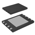
290 Uses0 StarsW25Q128JVPIQ
SPI Flash Memory with Dual/Quad SPI The W25Q128JV (128M-bit) Serial Flash memory provides a storage solution for systems with limited space, pins and power. The 25Q series offers flexibility and performance well beyond ordinary Serial Flash devices. They are ideal for code shadowing to RAM, executing code directly from Dual/Quad SPI (XIP) and storing voice, text and data. The device operates on a single 2.7V to 3.6V power supply with current consumption as low as 1µA for power-down. All devices are offered in space-saving packages. The W25Q128JV array is organized into 65,536 programmable pages of 256-bytes each. Up to 256 bytes can be programmed at a time. Pages can be erased in groups of 16 (4KB sector erase), groups of 128 (32KB block erase), groups of 256 (64KB block erase) or the entire chip (chip erase). The W25Q128JV has 4,096 erasable sectors and 256 erasable blocks respectively. The small 4KB sectors allow for greater flexibility in applications that require data and parameter storage. (See Figure 2.) The W25Q128JV supports the standard Serial Peripheral Interface (SPI), Dual/Quad I/O SPI: Serial Clock, Chip Select, Serial Data I/O0 (DI), I/O1 (DO), I/O2 and I/O3. SPI clock frequencies of W25Q128JV of up to 133MHz are supported allowing equivalent clock rates of 266MHz (133MHz x 2) for Dual I/O and 532MHz (133MHz x 4) for Quad I/O when using the Fast Read Dual/Quad I/O. These transfer rates can outperform standard Asynchronous 8 and 16-bit Parallel Flash memories. New Family of SpiFlash Memories – W25Q128JV: 128M-bit / 16M-byte – Standard SPI: CLK, /CS, DI, DO – Dual SPI: CLK, /CS, IO0, IO1 – Quad SPI: CLK, /CS, IO0, IO1, IO2, IO3 – Software & Hardware Reset(1) Highest Performance Serial Flash – 133MHz Single, Dual/Quad SPI clocks – 266/532MHz equivalent Dual/Quad SPI – 66MB/S continuous data transfer rate – Min. 100K Program-Erase cycles per sector – More than 20-year data retention Efficient “Continuous Read” – Continuous Read with 8/16/32/64-Byte Wrap – As few as 8 clocks to address memory – Allows true XIP (execute in place) operation Low Power, Wide Temperature Range – Single 2.7 to 3.6V supply – <1µA Power-down (typ.) – -40°C to +85°C operating range – -40°C to +105°C operating range Flexible Architecture with 4KB sectors – Uniform Sector/Block Erase (4K/32K/64K-Byte) – Program 1 to 256 byte per programmable page – Erase/Program Suspend & Resume Advanced Security Features – Software and Hardware Write-Protect – Power Supply Lock-Down – Special OTP protection – Top/Bottom, Complement array protection – Individual Block/Sector array protection – 64-Bit Unique ID for each device – Discoverable Parameters (SFDP) Register – 3X256-Bytes Security Registers with OTP locks – Volatile & Non-volatile Status Register Bits Space Efficient Packaging – 8-pin SOIC 208-mil – 16-pin SOIC 300-mil (additional /RESET pin) – 8-pad WSON 6x5-mm / 8x6-mm – 24-ball TFBGA 8x6-mm (6x4/5x5 ball array) – 24-ball WLCSP – Contact Winbond for KGD and other options #CommonPartsLibrary #IntegratedCircuit #Memory
73 Uses0 StarsMAX98357AETE+T
Tiny, Low-Cost, PCM Class D Amplifier with Class AB Performance The MAX98357AETE+T is a highly integrated digital input Class-D audio amplifier designed to convert digital audio streams directly into high-efficiency speaker output signals. It features an integrated digital-to-analog conversion stage and Class-D output driver, eliminating the need for an external DAC and significantly simplifying audio system design. The device accepts digital audio data through a standard I²S interface and delivers high-quality audio output suitable for portable electronics, smart speakers, embedded systems, Internet of Things devices, multimedia products, and consumer audio equipment. Its high-efficiency architecture minimizes power dissipation while maintaining excellent audio performance, making it particularly suitable for battery-powered applications. The MAX98357AETE+T incorporates advanced audio processing capabilities, low electromagnetic interference characteristics, and integrated protection features to ensure reliable operation in compact embedded audio designs. Features Digital input Class-D audio amplifier Integrated digital-to-analog conversion functionality Direct I²S audio interface support High-efficiency power amplification architecture Filterless output design Compact surface-mount package Low electromagnetic interference operation Integrated click-and-pop suppression Low power consumption High audio fidelity performance Simplified external component requirements Integrated thermal protection Short-circuit protection capability Suitable for mono speaker applications Optimized for embedded audio systems Electrical Characteristics Digital audio input architecture Class-D switching amplifier topology High-efficiency power conversion Low distortion audio reproduction Wide operating supply range Low standby power consumption Direct speaker drive capability Integrated audio signal processing functions Applications Smart speakers Embedded audio systems Internet of Things devices Portable electronics Voice-enabled products Multimedia equipment Consumer audio devices Wireless audio products Home automation systems Educational and development platforms Battery-powered audio applications Human-machine interface systems Package Information TQFN surface-mount package Compact footprint for space-constrained designs Suitable for automated PCB assembly Thermally optimized package construction High-density electronic product integration #commonpartslibrary #integratedcircuit #audio #audioamplifier #classd amplifier #digitalaudio #i2s #dac #embeddedaudio #consumerelectronics #iot #multimedia #signalprocessing #powermanagement #maximintegrated #analogdevices #electronicsdesign #audioelectronics #speakerdriver #embeddedsystems
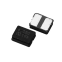
134 Uses0 StarsNX3225GD 8.000MHZ STD-CRA-3
The NX3225GD 8.000MHz STD-CRA-3 is a surface-mount quartz crystal resonator designed to provide a stable and accurate clock reference for electronic circuits. It is housed in a compact ceramic package suitable for space-constrained applications and is optimized for low power consumption and reliable frequency generation. This crystal is commonly used in microcontrollers, wireless communication modules, industrial control systems, consumer electronics, IoT devices, and embedded systems requiring precise timing and frequency control. Features Fundamental mode quartz crystal resonator Nominal frequency of 8.000 MHz Compact surface-mount ceramic package High frequency stability and accuracy Low equivalent series resistance Suitable for low-power oscillator circuits Excellent aging characteristics RoHS-compliant construction Designed for automated SMT assembly processes Reliable operation across industrial temperature environments Electrical Characteristics Crystal type: Quartz Crystal Resonator Frequency: 8.000 MHz Oscillation mode: Fundamental Load capacitance: Standard load capacitance configuration Frequency tolerance: Standard precision grade Frequency stability: Industrial-grade stability performance Equivalent series resistance optimized for MCU and RF oscillator circuits Low drive level operation High insulation resistance Mechanical Characteristics Surface-mount package Ceramic hermetic enclosure Compact footprint suitable for high-density PCB layouts Compatible with standard reflow soldering processes Designed for automated pick-and-place assembly Applications Microcontroller clock generation Wireless communication devices Bluetooth and RF modules IoT and smart devices Industrial automation equipment Embedded control systems Consumer electronics Timing and synchronization circuits Sensor interface modules Portable battery-powered products Compliance RoHS compliant Lead-free package Environmentally friendly manufacturing standards Suitable for commercial and industrial electronic applications #commonpartslibrary #crystal #quartzcrystal #frequencycontrol #timingdevice #clocksource #oscillator #smtcomponent #embeddedsystems #wirelesscommunication #industrialelectronics #consumerelectronics #iotdevices #passivecomponents #electroniccomponents
43 Uses0 StarsUSBLC6-2P6
ESD DIODE 5VWM 14VC SOT-666-6 The USBLC6-2P6 is a dual-line, rail-to-rail transient voltage suppressor (TVS) diode array in a compact SOT-666 package. It is specifically optimized for protecting USB D+ and D− lines (and similar high-speed differential pairs) while maintaining very low signal distortion due to its low capacitance design. It clamps high-voltage ESD events to safe levels, protecting sensitive ICs such as MCUs, USB PHYs, and transceivers. Designed for USB and high-speed data protection Ideal for USB 2.0 (480 Mbps) interfaces Very low line capacitance Minimizes signal distortion on high-speed differential pairs Bidirectional ESD protection Protects both positive and negative voltage transients Low clamping voltage Typical clamp around ~17 V during surge events High peak pulse current capability Handles ESD strikes (IEC 61000-4-2 compliant, typically ±15 kV air / ±8 kV contact in similar ST USBLC family devices) Rail-to-rail protection structure Protects signal lines relative to VCC and GND Compact SOT-666 package Suitable for very small PCB layouts (phones, USB ports, embedded systems) 2-channel configuration Typically used for D+ / D− pair protection Typical Applications USB 2.0 ports (D+ / D− protection) Smartphones and tablets Embedded systems with external connectors HDMI / Ethernet signal protection (low-capacitance variants also used) Any exposed high-speed data interface requiring ESD protection #CommonPartsLibrary #Diode
605 Uses0 StarsBQ25895MRTWR
I²C Controlled Single Cell Fast Charger with MaxCharge™ Technology for High Input Voltage and Adjustable Voltage 3.1A Boost Operation The bq25895M is a highly-integrated 5-A switchmode battery charge management and system power path management device for single cell Li-Ion and Lipolymer battery. The devices support high input voltage fast charging. The low impedance power path optimizes switch-mode operation efficiency, reduces battery charging time and extends battery life during discharging phase. The I 2C Serial interface with charging and system settings makes the device a truly flexible solution. • High Efficiency 1.5-MHz Switch Mode Buck Charge – 93% Charge Efficiency at 2 A and 91% Charge Efficiency at 3 A Charge Current – Optimize for High Voltage Input (9 V / 12 V) – Low Power PFM mode for Light Load Operations • Boost Mode Operation with Adjustable Output from 4.5 V to 5.5 V – Selectable 500-KHz / 1.5-MHz Boost Converter with up-to 3.1 A Output – 93% Boost Efficiency at 5 V at 1 A Output – Support down-to 2.5V Battery – Support PWM only or PFM/PWM control for Light Load Efficiency • Integrated Control to Switch Between Charge and Boost Mode • Single Input to Support USB Input and Adjustable High Voltage Adapters – Support 3.9-V to 14-V Input Voltage Range – Input Current Limit (100 mA to 3.25 A with 50- mA resolution) to Support USB2.0, USB3.0 standard and High Voltage Adapters – Maximum Power Tracking by Input Voltage Limit up-to 14V for Wide Range of Adapters – Auto Detect USB SDP, CDP, DCP, and Nonstandard Adapters • Input Current Optimizer (ICO) to Maximize Input Power without Overloading Adapters • Resistance Compensation (IRCOMP) from Charger Output to Cell Terminal • Highest Battery Discharge Efficiency with 11-mΩ Battery Discharge MOSFET up to 9 A • Integrated ADC for System Monitor (Voltage, Temperature, Charge Current) • BATFET Control to Support Ship Mode, Wake Up, and Full System Reset • Flexible Autonomous and I 2C Mode for Optimal System Performance • High Integration includes all MOSFETs, Current Sensing and Loop Compensation • 12-µA Low Battery Leakage Current to Support Ship Mode • High Accuracy – ±0.5% Charge Voltage Regulation – ±5% Charge Current Regulation – ±7.5% Input Current Regulation #CommonPartsLibrary #IntegratedCircuit #PowerManagement
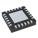
107 Uses0 StarsCP2102N-A02-GQFN24
USB-to-UART Bridge CP2102N-A02-GQFN24 is a highly integrated USB-to-UART bridge controller from Silicon Labs. It provides a simple and cost-effective way to add USB connectivity to embedded systems by converting USB 2.0 Full-Speed communication into a standard UART interface. The device integrates the USB transceiver, oscillator, voltage regulator, and UART controller, minimizing external components and eliminating the need for USB firmware development. It is commonly used in microcontroller programming interfaces, industrial equipment, POS terminals, data loggers, and USB-to-serial adapters. Key Features USB 2.0 Full-Speed compliant (12 Mbps) interface. USB-to-UART bridge with data rates up to 3 Mbaud. Integrated USB transceiver; no external USB resistors required. Integrated oscillator; no external crystal required. On-chip 3.3 V voltage regulator. USB Battery Charger Detection (BC 1.2) support. Remote wakeup capability from USB suspend state. Low operating current of approximately 9.5 mA. Hardware and software flow control support. Internal configurable ROM for Vendor ID, Product ID, serial number, and USB descriptors. Royalty-free Virtual COM Port (VCP) drivers available for major operating systems. Operating temperature range: −40°C to +85°C. Compact 24-pin QFN (4 mm × 4 mm) package. Typical Applications USB-to-Serial adapters Microcontroller programming and debugging interfaces Industrial automation equipment Point-of-sale (POS) terminals Medical instruments Data acquisition and logging systems Embedded systems requiring USB connectivity #commonpartslibrary #integratedcircuit
374 Uses0 Stars