Interface ICs
An interface IC is a type of integrated circuit that is designed to facilitate communication between two devices or systems. These devices are commonly used in electronic systems to enable the transfer of data and control signals between different components or subsystems. Some common use cases for interface ICs include connecting microcontrollers to peripherals such as sensors or displays, linking multiple processors together in a network, and enabling communication between devices using different communication protocols. Flux.ai has the world's largest community-driven public library of interface ICs, with footprints, symbols, datasheets, and simulation models. This library is a valuable resource for engineers and designers who need access to accurate and up-to-date information on these important components. Whether you are working on a new design project or simply looking to learn more about interface ICs, Flux.ai is an excellent resource to help you find the information you need.
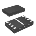
W25Q16JVUXIQ
SPI Flash Serial Flash Memory with Dual/Quad SPI The W25Q16JVUXIQ is a 16-Mbit (2-MByte) Serial NOR Flash memory device from Winbond. It is designed for embedded systems that require non-volatile code and data storage with minimal pin count, low power consumption, and high-speed access. The device supports standard SPI, Dual SPI, and Quad SPI interfaces, making it suitable for firmware storage, boot memory, IoT devices, microcontrollers, consumer electronics, and execute-in-place (XIP) applications. Key Features 16-Mbit (2-MByte) Flash Memory Capacity Operating Voltage: 2.7 V to 3.6 V Standard SPI, Dual SPI, and Quad SPI Interface Support Maximum SPI Clock Frequency: 133 MHz Equivalent Data Transfer Rates: 266 MHz (Dual SPI) 532 MHz (Quad SPI) Continuous Read and XIP (Execute-In-Place) Capability 4 KB Sector Erase, 32 KB Block Erase, 64 KB Block Erase, and Chip Erase 256-Byte Programmable Page Size Minimum 100,000 Program/Erase Cycles per Sector More Than 20 Years Data Retention Ultra-Low Power Consumption Typical power-down current below 1 µA 64-Bit Unique Serial Number Three 256-Byte Security Registers with OTP Protection JEDEC ID and SFDP Support Software and Hardware Write Protection Operating Temperature Options up to +85°C and +105°C Compact 8-Pad USON Package (2 mm × 3 mm) suitable for space-constrained designs #CommonPartsLibrary #IntegratedCircuit #Memory
167 Uses0 Stars91302-67-067R2M
M.2 CONN.P=0.5 6.7mm H conn The 91302-67-067R2M is a 67-position M.2 (NGFF) card-edge connector manufactured by UMAX. It is designed for connecting M.2 SSDs and PCIe-based expansion modules to a host PCB. The connector features an M-Key interface, making it suitable for high-speed PCIe storage applications such as NVMe solid-state drives. It is a surface-mount, right-angle receptacle with a 0.5 mm contact pitch and a 6.7 mm height above the PCB. Key Features M.2 M-Key connector Supports M-Key M.2 modules, commonly used for PCIe/NVMe SSDs. 67 contacts (67P) Standard pin count for M-Key M.2 card-edge connections. 0.5 mm pitch Fine-pitch design suitable for compact, high-density PCB layouts. Surface-mount, right-angle mounting Optimized for automated PCB assembly and low-profile system designs. 6.7 mm connector height Provides compatibility with standard M.2 card installation requirements. Female card-edge receptacle Accepts M.2 modules directly without additional adapters. RoHS compliant Meets environmental requirements for lead-free electronic assemblies. Typical Applications NVMe SSD sockets PCIe M.2 storage devices Embedded computing systems Industrial PCs Networking equipment Edge AI and IoT gateways Single-board computers requiring M.2 expansion #CommonPartsLibrary #Connector
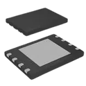
151 Uses0 StarsW25Q128JVPIQ
SPI Flash Memory with Dual/Quad SPI The W25Q128JV (128M-bit) Serial Flash memory provides a storage solution for systems with limited space, pins and power. The 25Q series offers flexibility and performance well beyond ordinary Serial Flash devices. They are ideal for code shadowing to RAM, executing code directly from Dual/Quad SPI (XIP) and storing voice, text and data. The device operates on a single 2.7V to 3.6V power supply with current consumption as low as 1µA for power-down. All devices are offered in space-saving packages. The W25Q128JV array is organized into 65,536 programmable pages of 256-bytes each. Up to 256 bytes can be programmed at a time. Pages can be erased in groups of 16 (4KB sector erase), groups of 128 (32KB block erase), groups of 256 (64KB block erase) or the entire chip (chip erase). The W25Q128JV has 4,096 erasable sectors and 256 erasable blocks respectively. The small 4KB sectors allow for greater flexibility in applications that require data and parameter storage. (See Figure 2.) The W25Q128JV supports the standard Serial Peripheral Interface (SPI), Dual/Quad I/O SPI: Serial Clock, Chip Select, Serial Data I/O0 (DI), I/O1 (DO), I/O2 and I/O3. SPI clock frequencies of W25Q128JV of up to 133MHz are supported allowing equivalent clock rates of 266MHz (133MHz x 2) for Dual I/O and 532MHz (133MHz x 4) for Quad I/O when using the Fast Read Dual/Quad I/O. These transfer rates can outperform standard Asynchronous 8 and 16-bit Parallel Flash memories. New Family of SpiFlash Memories – W25Q128JV: 128M-bit / 16M-byte – Standard SPI: CLK, /CS, DI, DO – Dual SPI: CLK, /CS, IO0, IO1 – Quad SPI: CLK, /CS, IO0, IO1, IO2, IO3 – Software & Hardware Reset(1) Highest Performance Serial Flash – 133MHz Single, Dual/Quad SPI clocks – 266/532MHz equivalent Dual/Quad SPI – 66MB/S continuous data transfer rate – Min. 100K Program-Erase cycles per sector – More than 20-year data retention Efficient “Continuous Read” – Continuous Read with 8/16/32/64-Byte Wrap – As few as 8 clocks to address memory – Allows true XIP (execute in place) operation Low Power, Wide Temperature Range – Single 2.7 to 3.6V supply – <1µA Power-down (typ.) – -40°C to +85°C operating range – -40°C to +105°C operating range Flexible Architecture with 4KB sectors – Uniform Sector/Block Erase (4K/32K/64K-Byte) – Program 1 to 256 byte per programmable page – Erase/Program Suspend & Resume Advanced Security Features – Software and Hardware Write-Protect – Power Supply Lock-Down – Special OTP protection – Top/Bottom, Complement array protection – Individual Block/Sector array protection – 64-Bit Unique ID for each device – Discoverable Parameters (SFDP) Register – 3X256-Bytes Security Registers with OTP locks – Volatile & Non-volatile Status Register Bits Space Efficient Packaging – 8-pin SOIC 208-mil – 16-pin SOIC 300-mil (additional /RESET pin) – 8-pad WSON 6x5-mm / 8x6-mm – 24-ball TFBGA 8x6-mm (6x4/5x5 ball array) – 24-ball WLCSP – Contact Winbond for KGD and other options #CommonPartsLibrary #IntegratedCircuit #Memory
38 Uses0 StarsBG95M3LA-64-SGNS
Cellular, Navigation BeiDou, EGDE, Galileo, GLONASS, GPS, GNSS, GSM, LTE Transceiver Module 850MHz, 900MHz, 1.8GHz, 1.9GHz Antenna Not Included Surface Mount The BG95M3LA-64-SGNS is a compact low-power LTE cellular communication module designed for IoT, telematics, asset tracking, industrial automation, and embedded wireless applications. The module supports global LTE Cat M1, Cat NB2, and EGPRS connectivity, enabling reliable wide-area wireless communication for battery-powered and mobile embedded systems. The device integrates cellular modem functionality, GNSS positioning capability, power management features, and multiple peripheral communication interfaces within a highly compact surface-mount package optimized for space-constrained embedded designs. The module is engineered for low-power operation, making it suitable for long-life IoT deployments requiring efficient wireless connectivity. The BG95M3LA-64-SGNS supports integrated satellite positioning technologies including GPS, GLONASS, Galileo, and BeiDou for location-aware applications. Its robust RF performance and industrial-grade operating capability allow deployment in harsh environmental conditions and demanding remote monitoring systems. The module provides comprehensive support for embedded communication protocols and is commonly used in smart meters, telematics units, industrial gateways, environmental monitoring systems, fleet tracking devices, and connected sensor platforms. Key Features LTE Cat M1 cellular communication support LTE Cat NB2 narrowband IoT capability EGPRS fallback connectivity Integrated GNSS positioning functionality Low-power optimized architecture Global wireless network compatibility Compact surface-mount module design Embedded TCP/IP protocol stack support UART, USB, and serial communication interfaces Integrated power management subsystem Industrial operating temperature support Embedded IoT connectivity optimization High-reliability wireless communication platform Multi-constellation satellite navigation support Electrical Characteristics Low operating power consumption Wide input voltage support High RF sensitivity performance Embedded low-power sleep functionality Stable wireless communication architecture Integrated RF and baseband processing Optimized antenna interface support Industrial-grade reliability performance Fast network registration capability Applications IoT and M2M communication systems Asset tracking devices Fleet management platforms Smart utility metering Industrial automation equipment Remote environmental monitoring Smart agriculture systems Telematics and transportation electronics Portable wireless data terminals Embedded gateway systems Smart city infrastructure Connected sensor platforms Package Information Package Type: LGA Module Mounting Type: Surface Mount Compact embedded wireless module package RoHS compliant configuration available #commonpartslibrary #wirelessmodule #lte #iot #embeddedhardware #cellularcommunication #gnss #telematics #industrialautomation #assettracking
106 Uses0 Stars