

USB4215-03-A
USB-C (USB TYPE-C) USB 2.0 Receptacle Connector 24 (16+8 Dummy) Position Surface Mount, Right Angle; Through Hole USB Type-C receptacle 16 pin USB2.0 The USB4215-03-A is a USB Type-C receptacle connector designed for USB 2.0 applications. It features a 16-pin configuration supporting reversible plug orientation with standard USB 2.0 differential data lines and configuration channel (CC) pins. The connector is intended for surface-mount PCB assembly with through-hole shell stakes for enhanced mechanical strength. It is widely used in compact embedded systems for power delivery, charging interfaces, and basic data communication. Key Features USB Type-C receptacle (USB 2.0 compliant) 16 functional pins (no SuperSpeed support) Reversible plug orientation Surface-mount contacts with through-hole shell tabs Compact, low-profile design High insertion cycle durability Suitable for automated assembly Electrical Characteristics Rated Current: VBUS: up to 5.0 A (depending on PCB design and cable) Signal pins: 0.25 A max Rated Voltage: 20 V DC max Contact Resistance: ≤ 40 mΩ Insulation Resistance: ≥ 100 MΩ Dielectric Withstanding Voltage: 100 V AC Mechanical Characteristics Mounting Type: Surface Mount (SMT) with Through-Hole Shield Tabs Number of Positions: 16 Mating Cycles: 10,000 cycles (typical) Insertion Force: 5–20 N Extraction Force: 8–20 N Material Specifications Contacts: Copper Alloy Contact Plating: Gold over Nickel Housing: High-temperature thermoplastic (UL94V-0) Shell: Stainless Steel Environmental Characteristics Operating Temperature Range: -25°C to +85°C Storage Temperature Range: -40°C to +85°C RoHS Compliant: Yes Halogen Free: Yes Pin Configuration (USB 2.0 Type-C) VBUS (Power) GND (Ground) D+ / D− (USB 2.0 differential pair) CC1 / CC2 (Configuration channel) SBU pins (optional/unused in USB 2.0 designs) Applications USB power input (5 V / USB-C PD trigger designs) Embedded systems and development boards Consumer electronics Charging interfaces Low-speed USB communication devices Packaging Tape & Reel for automated pick-and-place assembly Compliance & Standards USB Type-C Specification (USB 2.0 interface) RoHS / REACH compliant UL recognized materials #CommonPartsLibrary #Connector #USB-C... show more2.6k Uses
0 Stars
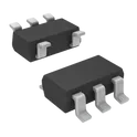
AP2112K-3.3TRG1
Linear Voltage Regulator IC Positive Fixed 1 Output 600mA SOT-25 3.3V LDO AP2112K-3.3 The AP2112K-3.3TRG1 is a low dropout (LDO) linear voltage regulator designed to provide a stable 3.3V output from a higher input voltage. It is optimized for low noise, high power supply rejection ratio (PSRR), and low quiescent current, making it suitable for battery-powered and noise-sensitive applications. The device features current limiting and thermal shutdown protection, ensuring reliable operation under fault conditions. It is commonly used in portable electronics, RF modules, microcontroller power supplies, and other low-power systems. Key Features Fixed output voltage: 3.3V Output current: up to 600 mA Low dropout voltage: ~250 mV at 300 mA load High PSRR: up to 70 dB at 1 kHz Low quiescent current: typically 55 µA Stable with low ESR ceramic capacitors Built-in overcurrent protection Thermal shutdown protection Fast transient response Absolute Maximum Ratings Input Voltage (VIN): up to 6.5 V Output Current: Internally limited Operating Junction Temperature: -40°C to +125°C Storage Temperature: -65°C to +150°C Electrical Characteristics (Typical values unless otherwise specified) Output Voltage Accuracy: ±2% Dropout Voltage: 250 mV @ 300 mA 400 mV @ 600 mA Line Regulation: 0.05%/V Load Regulation: 0.2% Quiescent Current: 55 µA Shutdown Current: <1 µA PSRR: 70 dB @ 1 kHz 45 dB @ 10 kHz Pin Configuration (SOT-23-5 / SC-70-5) VIN – Input voltage GND – Ground EN – Enable (active high) NC – No connection VOUT – Regulated output (3.3V) Package Information Package Type: SOT-23-5 (TRG1 suffix indicates tape & reel) Mounting: Surface mount Small footprint suitable for compact PCB layouts Typical Applications Battery-powered devices Wireless modules (Wi-Fi, Bluetooth, RF) Microcontroller and FPGA power supplies Portable consumer electronics Sensor and analog circuits requiring low noise Compliance & Reliability RoHS compliant Lead-free package Designed for high reliability and long operational life #CommonPartsLibrary #IntegratedCircuit #PowerManagement #LinearRegulator #VoltageRegulator... show more3.4k Uses
2 Stars

NE555P
The NE555 devices are precision timing circuits capable of producing accurate time delays or oscillation. In time-delay or monostable operating modes, the timed interval is controlled by a single external resistor and capacitor network. In the astable mode of operation, the frequency and duty cycle are controlled independently with two external resistors and a single external capacitor. Each timer has a trigger level equal to approximately one-third of the supply voltage and a threshold level equal to approximately two-thirds of the supply voltage. These levels can be altered by use of the control voltage pin (CONT). When the trigger input (TRIG) is less than the trigger level, the flip-flop is set and the output goes high. If TRIG is greater than the trigger level and the threshold input (THRES) is greater than the threshold level, the flip-flop is reset and the output is low. The reset input (RESET) overrides all other inputs and is used to initiate a new timing cycle. If RESET is low, the flip-flop is reset and the output is low. Whenever the output is low, a lowimpedance path is provided between the discharge pin (DISCH) and the ground pin (GND). Tie all unused inputs to an appropriate logic level to prevent false triggering. The output circuit is capable of sinking or sourcing current up to 200mA. Operation is specified for supplies of 5V to 15V. With a 5V supply, output levels are compatible with TTL inputs. Features - Timing from microseconds to hours - Astable or monostable operation - Adjustable duty cycle - TTL-compatible output can sink or source up to 200mA - On products compliant to MIL-PRF-38535, all parameters are tested unless otherwise noted. Applications - Pulse-shaping circuits - Missing-pulse detectors - Pulse-width modulators - Pulse-position modulators - Sequential timers - Pulse generators -F requency dividers - Industrial controls... show more2.4k Uses
1 Star
PTS636 SM43J SMTR LFS
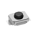
Tactile Switch SPST-NO Top Actuated Surface Mount. The PTS636 series is a small 6.0 x 3.5 form factor in SMT version with 3 different heights and 4 available actuation forces, ideal for general usage applications. It also included ground pin options on 2.5 mm height version.... show more1.5k Uses
0 Stars
TLV75533PDBVR
Linear Voltage Regulator IC Positive Fixed 1 Output 500mA SOT-23-5 The TLV75533PDBVR is a low-dropout (LDO) linear voltage regulator designed to provide a stable 3.3 V output from a higher input voltage source. It features ultra-low quiescent current and high power-supply rejection ratio (PSRR), making it ideal for battery-powered and noise-sensitive applications such as IoT devices, portable electronics, and RF circuits. The device is optimized for fast transient response and stable operation with small ceramic output capacitors. Key Features Fixed output voltage: 3.3 V Low dropout voltage (typ. ~200 mV at full load) Ultra-low quiescent current (typ. 25 µA) High PSRR for noise-sensitive applications Stable with small ceramic capacitors (≥1 µF) Thermal shutdown and overcurrent protection Available in compact SOT-23-5 package (DBV) Absolute Maximum Ratings Input voltage: –0.3 V to 6.5 V Output voltage: –0.3 V to (VIN + 0.3 V) Operating junction temperature: –40°C to +125°C Storage temperature range: –65°C to +150°C Recommended Operating Conditions Input voltage range: 1.45 V to 5.5 V Output voltage: 3.3 V (fixed) Output current: up to 500 mA Operating temperature range: –40°C to +125°C Electrical Characteristics (Typical unless otherwise noted) Output voltage accuracy: ±1% Dropout voltage: ~200 mV @ 500 mA Quiescent current: ~25 µA PSRR: up to 70 dB (at 1 kHz) Line regulation: <0.05%/V Load regulation: <0.5% Pin Configuration (SOT-23-5) Pin 1: IN – Input voltage Pin 2: GND – Ground Pin 3: EN – Enable (active high) Pin 4: NC – No connect Pin 5: OUT – Regulated output Typical Application Power management for microcontrollers and sensors Battery-powered portable devices RF and analog circuits requiring low noise supply IoT and wearable electronics Protection Features Thermal shutdown protection Overcurrent protection Undervoltage lockout (UVLO) #commonpartsLibrary #integratedcircuit #powermanagement #voltageregulator... show more525 Uses
0 Stars
TPS1HTC30-Q1
Automotive, 60-V, 6-A, 30-mΩ, one-channel smart high-side switch with adjustable current limit TPS1HTC30-Q1 is a single-channel, smart high-side switch, with integrated NMOS power FET and charge pump, designed to meet the requirements of 24-V automotive battery systems. The low RON(30 mΩ) minimizes device power dissipation driving a wide range of output load current up to 6-A DC, and the 60- V DC operating range improves system robustness. The device integrates protection features such as thermal shutdown, output clamp, and current limit. These features improve system robustness during fault events such as short circuit. TPS1HTC30-Q1 implements an adjustable current limiting circuit that improves the reliability of the system by reducing inrush current when driving large capacitive loads and minimizing overload current. The device also provides an accurate load current sense that allows for improved load diagnostics such as overload and open-load detection enabling better predictive maintenance. TPS1HTC30-Q1 is available in a small 14-pin, 4.40- mm × 5.0-mm HTSSOP leaded package with 0.65- mm pin pitch minimizing the PCB footprint. • Single-channel smart high-side power switch for 24-V automotive systems with full diagnostics • Wide operating voltage range: 6 V to 60 V – OVP protection: 66 V • Low RON: 30-mΩ typical, 55-mΩ maximum • Low standby current: < 0.5 µA • Low quiescent current (Iq): < 2 mA • Improve system level reliability through adjustable current limiting – Current limit: 2 A –16 A • Accurate current sensing: ±4% at 1 A • Protection – Overload and short-circuit protection – Integrated inductive discharge clamp – Undervoltage lockout (UVLO) protection – Loss of GND, loss of supply protection – Reverse battery protection with external components • Diagnostics – On and off state output open-load and short-tobattery detection – Overload and short to ground detection – Absolute and relative thermal shutdown detection • Functional Safety-Capable – Documentation available to aid functional safety system design • Operating junction temperature: –40 to 125°C • Input control: 1.8-V, 3.3-V and 5-V logic compatible • Integrated fault sense voltage scaling for ADC protection • Qualifications – AEC-Q100 qualified for automotive applications • Temperature grade 1: –40°C to +125°C, TA • 14-pin thermally-enhanced TSSOP package TPS1HTC30AQPWPRQ1 #CommonPartsLibrary #IntegratedCircuit... show more218 Uses
0 Stars
CMA-4544PF-W
20 Hz ~ 20 kHz Analog Microphone Electret Condenser 3 V ~ 10 V Omnidirectional (-44dB ±2dB) PC Pins JLI 140A HD microphone microphone capsule The CMA-4544PF-W is an electret condenser microphone designed for compact audio capture applications. It features high sensitivity, low noise characteristics, and stable frequency response, making it suitable for voice recording, communication devices, and embedded audio systems. The device integrates a permanently charged electret diaphragm with a built-in FET preamplifier, enabling reliable signal output with minimal external circuitry. Key Features Electret condenser microphone element High sensitivity and signal-to-noise ratio Omnidirectional pickup pattern Compact, low-profile package Built-in FET impedance converter Stable performance over temperature range RoHS compliant Electrical Characteristics Operating Voltage: typically 2.0 V (range: 1.5 V to 10 V) Current Consumption: typically 0.5 mA Sensitivity: typically -44 dB ±3 dB (at 1 kHz, 0 dB = 1 V/Pa) Signal-to-Noise Ratio: typically 60 dB Output Impedance: typically 2.2 kΩ Frequency Response: 20 Hz to 16 kHz Acoustic Characteristics Directivity: Omnidirectional Maximum Sound Pressure Level: typically 110 dB SPL Equivalent Noise Level: typically 34 dB SPL Mechanical Characteristics Package Type: Through-hole cylindrical metal can Dimensions: approximately 4.5 mm diameter × 4.4 mm height Mounting Type: PCB through-hole Terminal Configuration: Two-pin (signal and ground) Environmental Specifications Operating Temperature Range: -20°C to +70°C Storage Temperature Range: -40°C to +85°C Applications Voice recording devices Mobile and handheld electronics Intercom and communication systems Embedded audio input modules IoT and consumer electronics Pin Configuration Pin 1: Output (Vout) Pin 2: Ground (GND / Case) Compliance RoHS compliant Suitable for general consumer electronics use #commonpartslibrary #audio #microphone #analog #condenser... show more76 Uses
0 Stars
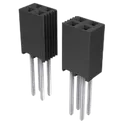
SSQ-110-03-T-D
20 Position Receptacle Connector 0.100" (2.54mm) Through Hole Tin The SSQ-110-03-T-D is a through-hole dual-row socket strip receptacle connector manufactured by Samtec, designed for board-to-board and pin header mating applications using the industry-standard pitch spacing that has been dominant in through-hole PCB interconnect design for decades. It belongs to Samtec's SSQ series, a family of square-post socket strip connectors that accept standard square-pin headers and are widely used across prototyping, instrumentation, test and measurement, embedded systems, industrial control, and general-purpose PCB stacking applications. As a socket strip of the receptacle gender, the SSQ-110-03-T-D is intended to receive a mating male pin header, creating a reliable and separable board-to-board or wire-to-board connection. The dual-row configuration provides a higher contact density within a given board length than a single-row socket, which is why dual-row socket strips in this pitch class are extensively used in applications such as microcontroller and single-board computer expansion connectors, module-to-baseboard interfaces, and other designs where a significant number of signal, power, or ground connections must be made across a single separable connector interface. The connector features square solder tails for through-hole PCB mounting, with the "-T" suffix in the part number designating the square post tail style, which provides a well-defined mechanical footprint and reliable solder joint formation in wave solder and hand-solder assembly processes. The "-D" suffix indicates the dual-row configuration. Contact material is phosphor bronze, a widely used spring-contact alloy chosen for its combination of good electrical conductivity, excellent spring properties that maintain consistent contact force across many mating cycles, and resistance to stress relaxation over time. The contacts are finished with matte tin plating over nickel underplate, providing a solderable, cost-effective contact surface suitable for the majority of general-purpose signal and low-power applications for which this connector class is typically used. The insulator body is molded from black liquid crystal polymer, a high-performance engineering thermoplastic that offers the high dimensional stability, excellent electrical insulation properties, and high-temperature resistance needed to withstand wave soldering and reflow-adjacent thermal exposure during PCB assembly. The material also carries a UL94 V-0 flammability rating, reflecting its self-extinguishing behavior in the event of an ignition source, which is required or preferred in many end-product regulatory compliance frameworks. The SSQ series is widely used in conjunction with Samtec's TSW series male pin headers as a complementary mating pair, and the connector is compatible with a broad range of standard square-pin headers from other manufacturers that conform to the same pitch and pin geometry, making it a versatile choice for general-purpose through-hole header applications. Spec Sheet Identification Part Number: SSQ-110-03-T-D Series: SSQ Manufacturer: Samtec, Inc. Connector Type / Configuration Type: Socket strip receptacle Gender: Female (receptacle) Row Configuration: Dual row Orientation: Straight, vertical Mounting Method: Through-hole, solder tail Contact & Material Properties Contact Material: Phosphor bronze Contact Finish — Mating Zone: Matte tin over nickel Contact Finish — Post/Tail: Tin Contact Type: Forked socket, square post acceptance Post/Tail Style: Square solder tail Mechanical Specifications Contact Pitch: Standard pitch class, widely used through-hole spacing Profile Height: Standard SSQ series mated height class Insulator Color: Black Insulator Material: Liquid crystal polymer (LCP) Flammability Rating: UL94 V-0 Body Orientation: Straight Electrical Ratings Current Rating Per Contact: Mid-range per-pin current class Voltage Rating: High AC and DC voltage rating class for general-purpose signal use Mating Cycles: Rated for repeated mate/unmate cycles Environmental & Qualification Operating Temperature Range: Extended range, suitable for industrial environments RoHS Compliance: Yes Export Classification: EAR99 Mating Compatibility Mates With: Samtec TSW series male pin headers and compatible standard square-pin headers from other manufacturers Application Note: Suitable for board-to-board stacking, module-to-baseboard interfaces, SBC expansion connectors, and general-purpose through-hole header applications Packaging Supply Format: Bulk packaging #SSQ110 #Samtec #SocketStrip #DualRowConnector #ThroughHoleConnector #PCBReceptacle #PinHeader #BoardToBoard #FemaleSockets #PhosphorBronze #LCP #UL94V0 #EmbeddedSystems #Prototyping #InstrumentationConnector #GeneralPurposeConnector #ConnectorDatasheet #EngineeringSpec #ComponentLibrary #CommonPartsLibrary #RoHSCompliant #PCBDesign #CommonPartsLibrary #Connector #Header #Receptacle #Female-Socket #SSQ... show more35 Uses
0 Stars
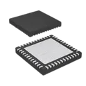
NRF52840-QFAA-F-R
IC RF TxRx + MCU 802.15.4, Bluetooth Bluetooth v5.0, Thread, Zigbee® 2.4GHz 48-VFQFN Exposed Pad The NRF52840-QFAA-F-R belongs to Nordic’s nRF52 series and supports multiple wireless standards including Bluetooth 5, Bluetooth Low Energy (BLE), Thread, Zigbee, ANT, and proprietary 2.4 GHz protocols. It features a 64 MHz ARM Cortex-M4F CPU with floating-point unit (FPU), making it suitable for both wireless communication and real-time embedded processing. The device integrates large memory resources, rich peripherals, USB support, NFC capability, and advanced security features, reducing the need for external components in wireless embedded designs. Key Features 32-bit ARM Cortex-M4F processor running at 64 MHz 1 MB Flash memory and 256 KB RAM Supports Bluetooth 5 / BLE, Thread, Zigbee, ANT, and proprietary 2.4 GHz protocols IEEE 802.15.4 compliant radio Up to +8 dBm TX output power High receiver sensitivity down to −103 dBm Data rates up to 2 Mbps Ultra-low power consumption for battery-powered applications USB 2.0 Full-Speed controller NFC-A tag support Multiple communication interfaces: SPI UART I2C (TWI) I2S PWM PDM ADC Up to 48 GPIOs Integrated ARM CryptoCell-310 security engine Operating voltage range: 1.7 V to 5.5 V Operating temperature: −40°C to +85°C Compact 48-QFN (6×6 mm) package Typical Applications BLE devices Smart home products Wearables Wireless sensors Industrial IoT HID devices (keyboard/mouse) Asset tracking Mesh networking devices USB dongles and gateways PCB Design Notes Community PCB reviews commonly recommend: Proper RF grounding and 50-ohm antenna routing Using ESD/TVS protection on USB lines Keeping RF matching components close to the antenna Using solid ground planes for 2.4 GHz performance #CommonPartsLibrary #IntegratedCircuit #RF... show more28 Uses
0 Stars
LM339ANSR
The LM339B and LM2901B devices are the next generation versions of the industry-standard LM339 and LM2901 comparator family. These next generation B-version comparators feature lower offset voltage, higher supply voltage capability, lower supply current, lower input bias current, lower propagation delay, and improved 2 kV ESD performance and input ruggedness through dedicated ESD clamps. The LM339B and LM2901B can drop-in replace the LM239, LM339 and LM2901, for both "A" and "V" grades. All devices consist of four independent voltage comparators that are designed to operate from a single power supply over a wide range of voltages. Quiescent current is independent of the supply voltage. • NEW LM339B and LM2901B • Improved specifications of B-version – Maximum rating: up to 38V – ESD rating (HBM): 2kV – Low input offset: 0.37mV – Low input bias current: 3.5nA – Low supply-current: 200µA per comparator – Faster response time of 1µsec – Extended temperature range for LM339B • B-version is drop-in replacement for LM239, LM339 and LM2901, A and V versions • Common-mode input voltage range includes ground • Differential input voltage range equal to maximumrated supply voltage: ±38V • Low output saturation voltage • Output compatible with TTL, MOS, and CMOS • For single version, see the TL331B • For dual version, see the LM393B or LM2903B #CommonPartsLibrary #IntegratedCircuit #Comparator... show more56 Uses
0 Stars
SEAM-40-01-L-10-2-RA-K-TR
Board to Board & Mezzanine Connectors .050\" SEARAY High-Speed High-Density Open-Pin-Field Array Terminal 400 Position Connector High Density Array, Male Surface Mount, Right Angle Gold SEAM-40-01-L-10-2-RA-K-TR is a high-speed, high-density board-to-board mezzanine connector from the Samtec SEARAY™ series. It features a right-angle, surface-mount design with 400 positions arranged in a 10-row open-pin-field array on a 1.27 mm (0.050") pitch. The connector utilizes Samtec's Edge Rate® contact system, providing excellent signal integrity, durability, and support for high-speed differential pair routing in demanding communication, networking, and embedded computing applications. Key Features High-density 400-position open-pin-field array connector 1.27 mm (0.050") contact pitch for compact board-to-board interconnects Right-angle, surface-mount termination Rugged Edge Rate® contact system for reliable high-speed performance Supports high-speed serial protocols and differential pair routing Suitable for power, ground, and signal connections within the same connector Gold-plated contacts for enhanced reliability and corrosion resistance Board-guide feature for improved mating alignment Current rating up to 1.9 A per contact Voltage rating up to 240 VAC / 339 VDC Tape-and-reel packaging for automated assembly processes RoHS compliant and designed for high-reliability applications #Samtec #SEARAY #SEAM4001L102RAKTR #BoardToBoardConnector #MezzanineConnector #HighSpeedConnector #HighDensityInterconnect #EdgeRate #SurfaceMount #RightAngleConnector #EmbeddedSystems #TelecomEquipment #NetworkingHardware #IndustrialElectronics #PCBDesign... show more1 Use
0 Stars
VNI2140J
Power Switch/Driver 1:1 N-Channel 500mA PowerSSO-12 8-channel protected high-side 12 V output switch IC The VNI2140J is a monolithic device designed using STMicroelectronics' VIPower technology. The device drives two independent resistive or inductive loads with one side connected to ground. Active current limitation prevents a drop in system power supply in cases of shorted-load, and built-in thermal shutdown protects the chip from damage due to overtemperature and short-circuit. In overload conditions, channel turns OFF and ON automatically to maintain the junction temperature between TTSD and TR. If the case temperature reaches TCSD, the overloaded channel is turned OFF and restarts only when case temperature decreases down to TCR. In order to avoid high-peak current from the supply, when more than one channel is overloaded the TCSD restart is not simultaneous. Non overloaded channels continue to operate normally. The open-drain diagnostics output indicates overtemperature conditions and open-load in OFF-state. Features • Nominal current: 0.75 A per channel • Shorted-load protections • Junction overtemperature protection • Case overtemperature protection for thermal independence of the channels • Thermal case shutdown restart not simultaneous for the various channels • Protection against loss of ground • Current limitation 1 A per channel • Undervoltage shutdown • Open-load in OFF-state and short to VCC detection • Open-drain diagnostic outputs • 3.3 V CMOS/TTL compatible inputs • Fast demagnetization of inductive loads • Conforms to IEC 61131-2 Applications • Programmable logic control • Industrial PC peripheral input/output • Numerical control machines #VNI2140J #STMicroelectronics #VIPower #HighSideSwitch #SolidStateRelay #PowerManagement #IndustrialAutomation #PLC #LoadDriver #PowerSSO12... show more18 Uses
0 Stars
MAX25432BATLG/V+
USB Type C PMIC 40-TQFN (6x6) The MAX25432 combines an automotive-grade buckboost controller capable of full-range 3.3V to 21V programmable power supply (PPS) at up to 6.35A, USB Power Delivery (USB PD) analog front-end (AFE), legacy USB charging support, and USB Type-C® protection switches for automotive USB host or downstream-facing (DFP) applications. The USB TypeC protection switches provide automotive system-level ESD protection and 24V short-circuit protection for D+, D-, CC1, CC2, and VCONN. The device can optionally support legacy charging modes for older passenger phones including BC1.2, Apple® Charge, Apple CarPlay®, Apple MFi, and USB On-The-Go (OTG). The MAX25432B integrates a USB PD AFE, which supports the USB-IF Type-C Port Controller Interface (TCPCI) specification and can interface with any I2C controller in the application. The MAX25432A provides configuration channel (CC) signal pass-through protection for an external USB PD controller. P-suffix and G-suffix devices include intelligent detection and protection to avoid high short-circuit currents flowing from the car battery through the cable shield to ground during fault events, thus preventing car module damage. The MAX25432 is available in a small, 6mm x 6mm, 40- pin TQFN-EP package and requires very few external components. The MAX25432 evaluation (EV) kit and collateral provide a convenient platform to the design engineer for rapid evaluation with reduced test and firmware development time. Integrated I2C Buck-Boost Controller with PPS 4.5V to 36V Input Operating Range 3.3V to 21V Constant Voltage, 10mV LSB 1A to 6.35A Current Limit, 25mA LSB 220kHz, 300kHz, and 400kHz SwitchingFrequency VBUS Cable Compensation up to 516mΩ External Frequency Synchronization and SpreadSpectrum for Reduced EMI USB PD 3.1 Type-C Port Controller USB-IF Compliant - TID 9154 Up to 800mV Ground Offset Pairs with ADI TCPM for Turn-Key Solution MAX25432BATLP Enables: ADI TCPM Alternate Mode and Dual-Role Port Improved CC Detection Advanced Monitoring Algorithms (V, T) Dynamic Loop Control Highest Performance, Safest, and Lowest Cost Passenger Cable-Shield Short-to-Battery Protection Minimizes Short-Circuit Currents with a Small,Single-FET Solution Integrated Current-Sense Amplifiers, ADC and DAC Integrated 3.3V to 5.0V, 1.5W, Smart, Reliable VCONN Switches and Protection, 50mA to 500mA OCP Integrated 24V DC Protection on Protected HVD+, HVD-, HVCC1, HVCC2 Outputs Integrated Legacy USB 2.0 Charging Support Including BC1.2, Apple CarPlay, OTG, and Apple MFi Rev 3x Integrated ±15kV Air-Gap/±8kV Contact Discharge ISO 10605 and IEC 61000-4-2 ESD Protection -40°C to +125°C Operating Temperature Range 40-Pin, 6mm x 6mm, TQFN Package with EP AEC-Q100 and AEC-Q006 Qualified #CommonPartsLibrary #IntegratedCircuit #PowerManagement... show more17 Uses
0 Stars
STISO621WTR
General Purpose Digital Isolator 5000Vpk 2 Channel 100Mbps 50kV/µs CMTI 8-SOIC (0.295", 7.50mm Width) General Description The STISO621WTR is a high-performance quad-channel isolated digital input interface IC from STMicroelectronics. It is designed to interface industrial digital inputs (such as PLC inputs) with low-voltage logic systems while providing galvanic isolation for improved safety and noise immunity. This device integrates four independent input channels, each capable of handling high-voltage input signals, and converts them into isolated logic-level outputs. It is ideal for industrial automation, programmable logic controllers (PLCs), and factory control systems where robust signal isolation is required. Key Features Quad isolated digital input channels High common-mode transient immunity (CMTI) Wide input voltage range for industrial signals Integrated current limiting and protection circuitry Compatible with 3.3V and 5V logic outputs Low power consumption High noise immunity and ESD robustness Complies with industrial safety standards Electrical Characteristics Number of Channels: 4 Isolation Type: Galvanic isolation Input Voltage Range: Up to ~30 V (industrial input level) Logic Output Voltage: 3.3 V / 5 V compatible Propagation Delay: Typically low (tens of ns range) Supply Voltage (Vcc): 3.0 V to 5.5 V Operating Temperature Range: -40°C to +125°C Functional Description Each input channel accepts a high-voltage industrial signal and converts it into a corresponding isolated digital output. Internal circuitry provides: Input current limiting Signal conditioning Isolation barrier Output buffering The isolation barrier protects low-voltage control electronics from high-voltage transients, ground loops, and electrical noise. Package Information Package Type: SO-16 (Wide body) Mounting: Surface-mount (SMD) Tape & Reel: Yes (TR suffix) Pin Count: 16 pins Applications Programmable Logic Controllers (PLC) Industrial I/O modules Factory automation systems Motor control interfaces Process control equipment Building automation Advantages Eliminates need for external optocouplers Reduces PCB space and BOM cost Improves system reliability High-speed digital isolation vs traditional opto-isolators Compliance & Standards Industrial-grade reliability ESD protection compliant RoHS compliant Manufacturer Information Manufacturer: STMicroelectronics Part Number: STISO621WTR Series: STISO #commonpartslibrary #isolator... show more17 Uses
0 Stars
M24256E-FMN6TP
EEPROM Memory IC 256Kbit I2C 1 MHz 450 ns 8-SO The M24256E-FMN6TP is a 256-Kbit (32 Kbyte) I²C-compatible serial EEPROM from STMicroelectronics. It is designed for reliable, non-volatile data storage in a wide range of electronic applications including consumer, industrial, and automotive systems. The device supports standard (100 kHz), fast (400 kHz), and fast-mode plus (1 MHz) I²C communication, enabling efficient data transfer. It features byte and page write operations, low power consumption, and a high endurance of write cycles, making it suitable for frequent data logging and configuration storage. Housed in a compact SO8 package, the device is optimized for space-constrained PCB designs while maintaining robust performance and data retention capabilities. Key Features Memory size: 256 Kbit (32 Kbyte) Interface: I²C (2-wire serial interface) Clock frequency: Standard mode: 100 kHz Fast mode: 400 kHz Fast-mode Plus: 1 MHz Supply voltage range: 1.7 V to 5.5 V Page write capability: up to 64 bytes Write cycle time: ~5 ms (typical) Data retention: > 200 years Endurance: > 4 million write cycles Hardware write protection available ESD protection and latch-up immunity Functional Description The device operates as a slave on the I²C bus and supports: Byte write and read Page write (up to 64 bytes) Random and sequential read operations Memory addressing is internally managed using a 16-bit address pointer, allowing access to the full 32 KB memory array. The device includes an internal write cycle controller, eliminating the need for external timing management. Pin Configuration (SO8 Package) A0, A1, A2: Device address inputs VSS: Ground SDA: Serial data line SCL: Serial clock line WC: Write control (hardware write protection) VCC: Supply voltage Absolute Maximum Ratings Supply voltage (VCC): -0.3 V to 6.5 V Input voltage: -0.3 V to VCC + 0.6 V Storage temperature: -65°C to +150°C Operating temperature (industrial grade): -40°C to +85°C Electrical Characteristics Low standby current: < 1 µA (typical) Operating current: < 1 mA Input/output compatible with CMOS logic levels Schmitt trigger inputs for noise immunity Timing Characteristics Write cycle time: 5 ms (typical) Fast-mode Plus support up to 1 MHz Sequential read supports continuous data streaming Package Information Package type: SO8 (8-lead Small Outline) Mounting: Surface-mount (SMD) Tape & reel packaging (TP suffix) Applications Configuration storage Calibration data storage Data logging systems Industrial control systems Consumer electronics Embedded systems requiring non-volatile memory Advantages High endurance and long data retention Wide voltage range (ideal for mixed-voltage systems) Compact footprint High-speed I²C compatibility (up to 1 MHz) #commonpartslibrary #integratedcircuit #memory... show more16 Uses
0 Stars
5106081-1
77 (55 + 22 Ground) Position Header, Male Pins Connector 0.079" (2.00mm) Through Hole The 5106081‑1 is a high-reliability male PCB connector manufactured by TE Connectivity. It belongs to the Z‑PACK 2 mm HM Series, designed for mezzanine and backplane board-to-board interconnects. The connector features precision-machined phosphor bronze contacts with tin plating, ensuring consistent electrical conductivity, low contact resistance, and long-term reliability. The device has a through-hole press-fit termination style for robust mechanical attachment to printed circuit boards and optimal compatibility with automated assembly processes. Its vertical orientation and standardized 2 mm pitch allow compact, high-density PCB layouts while maintaining reliable alignment and mating with compatible female headers. The connector is engineered to support repeated insertion cycles, high signal integrity, and consistent electrical performance in industrial, telecommunications, and embedded electronic applications. General Description The 5106081‑1 is a durable, 77-position male PCB connector intended for high-density board-to-board interconnect solutions. It provides secure electrical connections, mechanical stability, and long-term reliability in demanding electronic systems. Widely used in industrial automation, telecommunications, and embedded computing, this connector ensures precise mating, easy PCB integration, and robust operation in backplane and mezzanine applications. Its press-fit through-hole design, reliable contact material, and standardized footprint make it a versatile solution for complex multi-board electronic assemblies. #TEConnectivity #PCBConnector #MaleHeader #BoardToBoard #ZPACK #2mmPitch #HighDensityInterconnect #ThroughHole #PressFit #IndustrialElectronics #Telecommunications #EmbeddedSystems #ElectricalEngineering #ReliableConnection #EngineeringSpec #ElectronicConnector #HighPerformanceConnector... show more2 Uses
0 Stars
QPA9442TR13
RF Amplifier IC 5G, TDD 600MHz ~ 2.8GHz 20-QFN (4x4) ## Engineering Specification ## General Description The **QPA9442TR13** is a Qorvo high-linearity RF pre-driver amplifier designed for wireless infrastructure, cellular communication systems, and high-performance RF transmit chain applications. It is intended for use in systems requiring wideband operation, strong linearity, stable gain performance, and compact surface-mount integration. The device is suitable for 5G, TDD, FDD, mobile infrastructure, massive MIMO, and general-purpose wireless designs. ## Device Identification Manufacturer Part Number: **QPA9442TR13** Manufacturer: **Qorvo** Device Category: **RF and Wireless Integrated Circuit** Device Type: **RF Amplifier** Functional Type: **High-Linearity RF Pre-Driver Amplifier** Application Class: **Wireless Infrastructure and 5G RF Front-End** ## Functional Description The device operates as a transmit-chain pre-driver amplifier, providing RF signal amplification before the final power amplification stage. It is designed to deliver high gain and high output linearity while supporting cellular-band tuning requirements. The amplifier includes shutdown control through a dedicated power-down function, allowing system-level power management in RF transmit applications. ## RF Performance Description The QPA9442TR13 supports wideband RF amplification for cellular and wireless infrastructure applications. It provides high linearity performance, strong compression-point capability, and output third-order intercept performance suitable for demanding transmit signal chains. The device is optimized for applications where signal quality, gain stability, and RF output performance are critical. ## Electrical Description The device is designed for single-supply operation and is suitable for low-voltage RF circuit designs. It requires proper RF matching, biasing, grounding, and thermal layout practices to achieve the intended performance. The part should be used according to the manufacturer’s recommended operating conditions and reference design guidance. ## Package and Mounting Description The component is supplied as a surface-mount RF integrated circuit in a compact QFN package with exposed pad construction. The package is intended for high-frequency printed circuit board layouts requiring controlled impedance routing, short RF signal paths, proper ground via placement, and effective thermal connection to the PCB ground plane. ## Protection and Control Features The amplifier includes internal RF overdrive protection and internal DC overvoltage protection. It also includes a DC power shutdown feature for power control and system-level enable or disable operation. ## Application Suitability The QPA9442TR13 is suitable for 5G base station equipment, massive MIMO radio systems, mobile infrastructure, TDD and FDD transmit systems, cellular RF front-end designs, general-purpose wireless equipment, and RF driver amplifier stages requiring high linearity and compact board-level integration. ## Design Considerations The device should be implemented with proper RF layout techniques, impedance-controlled traces, recommended matching networks, adequate grounding, and appropriate thermal management. Performance may vary depending on frequency tuning, PCB design, matching component selection, supply quality, and operating conditions. ## Hashtags #commonpartslibrary #integratedcircuit #rfamplifier #qorvo #qpa9442tr13 #qpa9442 #wirelesscomponents #rfic #semiconductor #electronicscomponents #rfdesign #wirelessinfrastructure #fiveg #tdd #fdd #massivemimo #mobileinfrastructure #preDriverAmplifier #rfpreDriver #smtcomponents #qfnpackage #pcbdesign #hardwaredesign #electronicsengineering #componentlibrary... show more0 Uses
0 Stars
USL00-30L-A
30 Position Connector Receptacle 0.016" (0.40mm) Surface Mount, Right Angle USL00-30L-A is a 30-position, 0.4 mm pitch right-angle receptacle connector from the KEL USL Series, designed for high-density connections using micro coaxial cables in compact electronic equipment. Its ultra-low profile design, reliable IDC termination, and multiple ground contacts make it suitable for high-speed signal transmission applications such as LCD panels, cameras, industrial electronics, and embedded systems. Key Features 30-position receptacle connector 0.4 mm contact pitch for high-density designs Right-angle surface-mount PCB mounting Ultra-low profile height of approximately 1.0 mm Designed for #42 AWG micro coaxial cables IDC (Insulation Displacement Contact) termination for reliable cable connection Multiple ground terminals for improved EMI/EMS performance Metal shell construction for enhanced shielding and mechanical strength Gold-plated contacts for reliable electrical performance Rated current: 0.25 A per contact Voltage rating: 200 VAC Operating temperature range: −40°C to +85°C Latch-lock mechanism for secure mating connection RoHS compliant and suitable for compact high-speed signal applications #KEL #USL0030LA #MicroCoaxConnector #BoardToCableConnector #FFCConnector #HighDensityConnector #SMTConnector #RightAngleConnector #EmbeddedSystems #IndustrialElectronics #SignalIntegrity #ElectronicComponents #PCBDesign #MicroCoax #InterconnectSolutions... show more0 Uses
0 Stars
B3U-1100PM
Tactile Switches Top Actuated Ground Tm w/out Boss 0.05A @ 12VDC #CommonPartsLibrary #switch #B3U... show more5 Uses
0 Stars
CC3-2412DF-E
Isolated Module DC DC Converter 2 Output 12 ~ 15V -12 ~ -15V 125mA, 125mA 18V - 36V Input The CC3-2412DF-E is an isolated DC-DC converter module designed to provide efficient and reliable power conversion in industrial, telecommunications, instrumentation, and embedded electronic systems. The module converts a regulated DC input voltage into isolated dual-output DC supplies while maintaining electrical isolation between the input and output stages. Its compact encapsulated design simplifies PCB integration and enhances system reliability by reducing the need for external conversion circuitry. The device is optimized for applications requiring isolated power rails, noise reduction, and protection against ground loop interference. Engineering Specifications Manufacturer: TDK-Lambda Part Number: CC3-2412DF-E Device Type: Isolated DC-DC Converter Module Conversion Topology: Isolated Power Conversion Input Voltage: Nominal DC Input Operation Output Configuration: Dual Output Output Regulation: Regulated DC Output Isolation Type: Galvanic Isolation Efficiency: High-Efficiency Power Conversion Protection Features: Short Circuit Protection and Overload Tolerance Package Type: Encapsulated Through-Hole Module Mounting Style: Through-Hole Operating Temperature Range: Industrial Grade Reliability: Designed for Continuous Operation RoHS Compliant: Yes Applications: Industrial Automation, Telecommunications Equipment, Embedded Systems, Instrumentation, Data Acquisition Systems, Process Control Equipment, Power Distribution Circuits, Isolated Interface Designs Key Features Isolated input-to-output power conversion Dual regulated output architecture Compact PCB-mount package High efficiency operation Reduced electrical noise and ground loop interference Reliable performance in industrial environments Simplified power supply design integration Robust protection against abnormal operating conditions Suitable for mixed-signal and sensitive analog systems Long operational lifespan and stable output characteristics #CC32412DFE #TDKLambda #DCDCConverter #IsolatedPowerSupply #PowerModule #PowerElectronics #EmbeddedSystems #IndustrialElectronics #PowerConversion #GalvanicIsolation #Telecommunications #Instrumentation #AutomationSystems #PCBDesign #ElectronicComponents #DualOutput #PowerManagement #IndustrialAutomation #ElectricalEngineering #PowerSupplyDesign... show more0 Uses
0 Stars










Page 1 of 4
Next