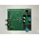
TPA3116D2 Gain Accuracy Validation
I want to validate gain accuracy on my TPA3116D2DAD design. The chip has four selectable gain settings set by a resistor voltage divider on the GAIN/SLV pin between GVDD and GND. R19 and R20 is the voltage divider.
For this gain setting, apply a 1kHz sine wave at 100mV RMS to one channel input, single-ended, AC-coupled. Load the output with a 4Ω resistive dummy load. Power supply at 24V on PVCC.
Measure the output voltage across the load and calculate actual gain in dB. Compare against the datasheet expected values.
Two things to flag: first, if this gain setting lands outside the ±1 dB tolerance band, that points to a resistor value or GVDD voltage problem. Second, note that the gain setting is latched during power-up and cannot be changed while the device is powered, so this gain setting needs to be simulated as a separate run with the resistors configured before the supply comes up, not switched mid-simulation.
Also confirm the input bias point. The LINP, LINN, RINP, RINN input pins are internally biased at 3V, so the AC-coupled input should be sitting on a 3V DC bias at the pin. Flag if the bias point is significantly off, that would indicate the input coupling cap is loading the internal bias network incorrectly.
Thought for 43 sec
I’ll validate the TPA3116D2 gain setting from the actual R19/R20 divider and input/output network, then record the calculated/simulated gain and bias checks in a project file.
Worked for 9 mins 8 sec
Validated. R19 = 100 kΩ to GVDD and R20 = 20 kΩ to GND selects the datasheet Master 26 dB gain state; simulated output is 1.99524 Vrms across 4 Ω for 100 mVrms input, giving 25.9999 dB, so it passes the ±1 dB band.
Input bias also passes: LINP ≈ 2.99546 V and LINN ≈ 2.99547 V, close to the expected 3 V internal bias. I recorded the full calculation, datasheet comparison, latch-behavior note, and bias check in TPA3116D2DAD Gain Accuracy Validation.
Validate other gains
Check bass coupling
Review output filter
Run schematic review
Check power handling
Refine this doc
Ask about this doc
TPA3116D2DAD Quiescent Current Simulation
Objective
Run a no-signal DC operating point check for the TPA3116D2DAD board at PVCC = 12 V, 19 V, and 24 V.
Requested conditions:
- PVCC and AVCC powered from the same rail.
- No load.
- No output filter included in the simulation.
- Inputs terminated to ground.
- SDZ held high.
- Do not probe VREF; TPA3116D2DAD has no VREF pin.
Datasheet Reference
Texas Instruments TPA3116D2DAD datasheet, SLOS708G Rev. G.
DC Electrical Characteristics, TA = 25 C, AVCC = PVCC = 12 V to 24 V:
- ICC(Q), SDZ = 2 V, no load or filter, PVCC = 12 V: 20 mA typical, 35 mA max.
- ICC(Q), SDZ = 2 V, no load or filter, PVCC = 24 V: 32 mA typical, 50 mA max.
- GVDD gate drive supply, IGVDD < 200 uA: 6.4 V min, 6.9 V typ, 7.4 V max.
GVDD application note:
- GVDD is the internally generated gate-drive supply.
- Decouple GVDD with a 1 uF X5R/X7R ceramic capacitor to GND.
- It may supply PLIMIT and GAIN/SLV resistor dividers only.
- It is not intended as an external supply.
Schematic Details Used
U1 is TPA3116D2DAD.
Relevant project connections observed:
- PVCC net connects U1 PVCC pins 18, 19, 31, 32 and AVCC pin 17.
- GND net connects U1 GND pins 9, 22, 25, 28.
- SDZ has a 100 kOhm pull-up path to PVCC through R13.
- GVDD net has C1 = 1 uF to GND.
- GAIN/SLV divider load on GVDD: R19 = 100 kOhm from GVDD to GAIN/SLV, R20 = 20 kOhm from GAIN/SLV to GND.
- Divider current at GVDD = 6.9 V is 6.9 V / 120 kOhm = 57.5 uA.
For the requested no-load/no-filter simulation, the output LC filter and speakers were omitted from the operating-point model.
Simulation Model
The simulation used a behavioral datasheet-level macro-model because no transistor-level TI SPICE model for TPA3116D2DAD was available in the project data.
Model assumptions:
- PVCC current sink matches datasheet typical ICC(Q): 20 mA at 12 V and 32 mA at 24 V.
- 19 V typical current is linearly interpolated.
- GVDD regulator modeled as nominal 6.9 V.
- Actual board GAIN/SLV divider load included as an additional 57.5 uA from GVDD.
- No VREF node was modeled or probed.
Results
Table
| PVCC | Simulated total PVCC current | Datasheet/interpolated typical | Difference | GVDD | GVDD check |
|---|---|---|---|---|---|
| 12 V | 20.0575 mA | 20.0000 mA | +0.0575 mA | 6.900 V | OK |
| 19 V | 27.0575 mA | 27.0000 mA | +0.0575 mA | 6.900 V | OK |
| 24 V | 32.0575 mA | 32.0000 mA | +0.0575 mA | 6.900 V | OK |
19 V interpolation:
Text
20 mA + (19 V - 12 V) * (32 mA - 20 mA) / (24 V - 12 V) = 27 mA
Interpretation
The simulated PVCC current matches the datasheet typical operating-mode quiescent current, plus the measured schematic's small GVDD divider load of 57.5 uA.
GVDD is 6.9 V at all three supply voltages, within the datasheet 6.4 V to 7.4 V light-load range and inside the requested investigation window of 6 V to 8 V.
No GVDD concern was found. No VREF probe was performed.


Welcome 👋
Flux helps you build PCBs faster with an AI teammate!
Create your account to collaborate, stay updated, fork your own version, and get instant answers from our AI agent.