TPA3116D2 Gain Accuracy Validation
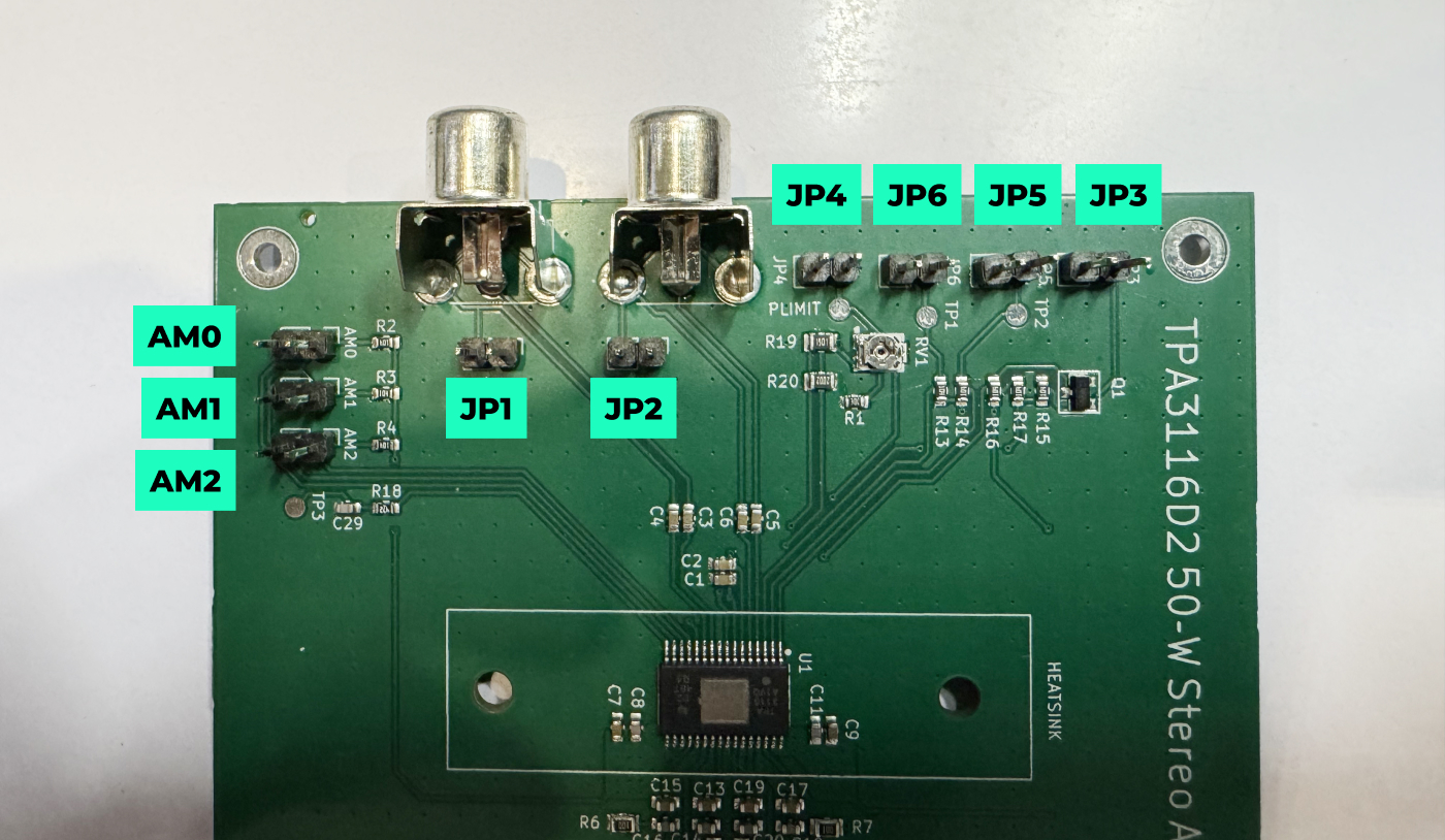
I want to validate gain accuracy on my TPA3116D2DAD design. The chip has four selectable gain settings set by a resistor voltage divider on the GAIN/SLV pin between GVDD and GND. R19 and R20 is the voltage divider.
For this gain setting, apply a 1kHz sine wave at 100mV RMS to one channel input, single-ended, AC-coupled. Load the output with a 4Ω resistive dummy load. Power supply at 24V on PVCC.
Measure the output voltage across the load and calculate actual gain in dB. Compare against the datasheet expected values.
Two things to flag: first, if this gain setting lands outside the ±1 dB tolerance band, that points to a resistor value or GVDD voltage problem. Second, note that the gain setting is latched during power-up and cannot be changed while the device is powered, so this gain setting needs to be simulated as a separate run with the resistors configured before the supply comes up, not switched mid-simulation.
Also confirm the input bias point. The LINP, LINN, RINP, RINN input pins are internally biased at 3V, so the AC-coupled input should be sitting on a 3V DC bias at the pin. Flag if the bias point is significantly off, that would indicate the input coupling cap is loading the internal bias network incorrectly.
Thought for 43 sec
I’ll validate the TPA3116D2 gain setting from the actual R19/R20 divider and input/output network, then record the calculated/simulated gain and bias checks in a project file.
Worked for 9 mins 8 sec
Validated. R19 = 100 kΩ to GVDD and R20 = 20 kΩ to GND selects the datasheet Master 26 dB gain state; simulated output is 1.99524 Vrms across 4 Ω for 100 mVrms input, giving 25.9999 dB, so it passes the ±1 dB band.
Input bias also passes: LINP ≈ 2.99546 V and LINN ≈ 2.99547 V, close to the expected 3 V internal bias. I recorded the full calculation, datasheet comparison, latch-behavior note, and bias check in TPA3116D2DAD Gain Accuracy Validation.
Validate other gains
Check bass coupling
Review output filter
Run schematic review
Check power handling
Refine this doc
Ask about this doc
Input, Output, Jumpers Settings
Image
Voltage input
Power enters through a 5.0 mm pitch terminal block and feeds the PVCC rail. The design includes large electrolytic bulk capacitors for local energy storage plus smaller bypass capacitors near the IC. That combination matters: the bulk caps help with low-frequency current demand, while the local ceramics handle the fast switching edges.
Expected safe power input: 12 V to 24 V DC. The TPA3116D2DAD amplifier IC is specified for 4.5 V to 26 V on PVCC / AVCC, so the board should be operated from a regulated DC supply that stays below 26 V at the amplifier supply pins, including tolerance, overshoot, and turn-on transients. The fitted 35 V bulk capacitors provide margin, but they do not raise the safe amplifier supply limit above 26 V.
Inputs
The left and right analog inputs use RCA jacks because they are familiar, easy to mount in an enclosure, and immediately recognizable to audio builders. The input path includes AC coupling so the amplifier does not depend on the source having a perfect DC offset.
Configuration jumpers
The board includes multiple jumpers and configuration nets for amplifier behavior. These make the design easier to remix because you can experiment with gain, modulation / mode selection, mute, shutdown, and mono-related wiring without rebuilding the entire schematic.
MODSEL jumper / JP5: This controls U1 pin 1, MODSEL, which selects the amplifier's Class-D switching behavior. When MODSEL is shorted to ground, the amplifier uses BD modulation, meaning balanced differential bridge switching. When MODSEL is pulled high, the amplifier uses 1SPW modulation, meaning 1-state pulse-width modulation, which reduces unnecessary switching at idle or low signal levels. This is not a power control; it changes the output switching mode.
SDZ jumper / JP6: This controls U1 pin 2, SDZ, the shutdown input. When SDZ is held high, the amplifier is enabled. When SDZ is shorted to ground, the amplifier enters shutdown: the outputs are muted / high impedance and the IC drops into a low-current state. This can behave like an electronic amp enable, standby, or mute control, but it does not disconnect the main PVCC power supply.
Left mono jumper / JP1: JP1 is the left-channel mono configuration jumper. It is part of the mono / PBTL setup path and should only be fitted when configuring the amplifier for the intended mono operating mode.
Right mono jumper / JP2: JP2 is the right-channel mono configuration jumper. It works with the mono / PBTL setup path and should be checked together with JP1 before running the amplifier in mono mode.
The mono / PBTL path is intentionally treated as a configuration mode. Before using the board in mono mode, verify the jumper state against the schematic and the TPA3116D2DAD datasheet. High-power mono operation is exactly where wiring mistakes become expensive.
Output stage
The board uses four 10 µH output inductors and four main output filter capacitors to form the LC filters after the Class-D switching outputs. This is the part of the design that turns high-frequency switching energy into something speaker-friendly.
The output network also includes small RC snubbers using low-value resistors and 0.01 µF capacitors. These are there to reduce ringing and make the output behavior cleaner, especially with real speaker cables and reactive loads.
RV1 power-limit trim: RV1 is an adjustable control for U1's PLIMIT pin. Adjusting RV1 changes the maximum output swing / power ceiling before the amplifier limits the output. It belongs with the output-stage behavior because it sets the amplifier's maximum allowed output power; it should be treated as a maximum-power trim, not a normal volume knob.


Welcome 👋
Flux helps you build PCBs faster with an AI teammate!
Create your account to collaborate, stay updated, fork your own version, and get instant answers from our AI agent.