TPA3116D2 Gain Accuracy Validation
I want to validate gain accuracy on my TPA3116D2DAD design. The chip has four selectable gain settings set by a resistor voltage divider on the GAIN/SLV pin between GVDD and GND. R19 and R20 is the voltage divider.
For this gain setting, apply a 1kHz sine wave at 100mV RMS to one channel input, single-ended, AC-coupled. Load the output with a 4Ω resistive dummy load. Power supply at 24V on PVCC.
Measure the output voltage across the load and calculate actual gain in dB. Compare against the datasheet expected values.
Two things to flag: first, if this gain setting lands outside the ±1 dB tolerance band, that points to a resistor value or GVDD voltage problem. Second, note that the gain setting is latched during power-up and cannot be changed while the device is powered, so this gain setting needs to be simulated as a separate run with the resistors configured before the supply comes up, not switched mid-simulation.
Also confirm the input bias point. The LINP, LINN, RINP, RINN input pins are internally biased at 3V, so the AC-coupled input should be sitting on a 3V DC bias at the pin. Flag if the bias point is significantly off, that would indicate the input coupling cap is loading the internal bias network incorrectly.
Thought for 43 sec
I’ll validate the TPA3116D2 gain setting from the actual R19/R20 divider and input/output network, then record the calculated/simulated gain and bias checks in a project file.
Worked for 9 mins 8 sec
Validated. R19 = 100 kΩ to GVDD and R20 = 20 kΩ to GND selects the datasheet Master 26 dB gain state; simulated output is 1.99524 Vrms across 4 Ω for 100 mVrms input, giving 25.9999 dB, so it passes the ±1 dB band.
Input bias also passes: LINP ≈ 2.99546 V and LINN ≈ 2.99547 V, close to the expected 3 V internal bias. I recorded the full calculation, datasheet comparison, latch-behavior note, and bias check in TPA3116D2DAD Gain Accuracy Validation.
Validate other gains
Check bass coupling
Review output filter
Run schematic review
Check power handling
Refine this doc
Ask about this doc
Comprehensive Block Diagram
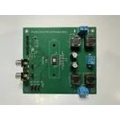
Project: High-Fidelity Class-D Audio Amplifier
This project is a TPA3116D2DAD-based analog-input Class-D amplifier. It accepts left and right analog audio inputs, amplifies them through a stereo Class-D power stage, filters each half-bridge output with LC output filters, and drives left and right speaker terminals. The design also includes supply decoupling, GVDD generation, PLIMIT control, mode and gain configuration, mute and shutdown control, fault indication, heatsinking, test points, and configuration jumpers for stereo or mono/PBTL-style use.
System Block Diagram
Diagram
Functional Blocks
1. Power Input and Distribution
- External supply enters through the 2-pin power connector J1 and duplicate PVCC/GND terminals.
- The PVCC net feeds U1 PVCC pins, AVCC, mode pullups, control pullups, and supply bypass capacitors.
- The GND net is the common return for the input network, amplifier grounds, output filter capacitors, bootstrap-related components, and power input return.
Main components:
- J1: power input connector
- +PVCC and GND terminals: alternate power entry or test access
- C10 and C12: 220uF bulk capacitors
- C7, C8, C9, C11 and smaller local capacitors: high-frequency decoupling
2. Audio Input Path
- The project has separate left and right RCA-style analog input connectors.
- Each input channel is AC-coupled into the TPA3116D2DAD differential input pins.
- Input jumpers allow the input configuration to be changed for stereo or mono-style operation.
Main components:
- L INPUT: left analog source connector
- R INPUT: right analog source connector
- C3 and C4: left input coupling capacitors
- C5 and C6: right input coupling capacitors
- JP1 and JP2: input configuration jumpers
- U1 pins LINP, LINN, RINP, RINN: differential audio inputs
3. Class-D Amplifier Core
- U1 is the central power amplifier IC: Texas Instruments TPA3116D2DAD.
- It accepts differential analog inputs and generates four switching half-bridge outputs.
- It includes internal gate-drive and protection functions, with external configuration through PLIMIT, gain, shutdown, mute, fault, mode select, AM avoidance, and sync pins.
Main component:
- U1: TPA3116D2DAD Class-D audio amplifier
4. GVDD, PLIMIT, and Gain Configuration
- U1 GVDD is locally bypassed by C1.
- PLIMIT is configured with a potentiometer and passive network to set the output power limit behavior.
- Gain and slave configuration are set by resistor straps tied to the GAIN/SLV pin.
Main components:
- C1: GVDD bypass capacitor
- RV1: PLIMIT trim potentiometer
- R1, C2: PLIMIT support network
- R19, R20: GAIN/SLV configuration resistors
5. Mode, Sync, AM Avoidance, Shutdown, Mute, and Fault Control
- AM0, AM1, AM2 and MODSEL are jumper-configured control inputs.
- SYNC is available through the sync network for switching-frequency synchronization or configuration.
- SDZ and MUTE are controlled by pullup/jumper networks.
- FAULTZ is exposed and connected into a transistor-based interface.
Main components:
- AM0, AM1, AM2 jumpers and associated 100k resistors
- JP4, JP5, JP6: mode, mute, and shutdown related jumpers
- R13, R14, R15, R16, R17, R18: control pull resistors
- Q1: MMBT2222A transistor used in the mute or fault interface
- FAULT, MUTE, SD, SYNC, MODESEL net portals and test access
6. Bootstrap and Switching Output Stage
- Each Class-D half-bridge has a bootstrap capacitor from the bootstrap pin to the switching output node.
- U1 outputs are OUTPL, OUTNL, OUTPR, and OUTNR.
- These switching nodes feed the LC output filters.
Main components:
- C13, C15, C17, C19: 0.22uF bootstrap capacitors
- U1 pins BSPL, BSNL, BSPR, BSNR
- U1 pins OUTPL, OUTNL, OUTPR, OUTNR
7. LC Output Filters and Speaker Outputs
- The four switching outputs are filtered by four 10uH inductors and associated capacitors/snubber networks.
- The filtered outputs drive the left and right speaker connectors and also route to individual LOUT/ROUT terminals.
Main components:
- L1, L2, L3, L4: 10uH output filter inductors
- C21, C22, C23, C24: 0.68uF filter capacitors
- C25, C26, C27, C28: 0.01uF filter or snubber capacitors
- C14, C16, C18, C20: 330pF snubber or EMI-control capacitors
- R9, R10, R11, R12: 3.3 ohm snubber resistors
- LEFT and RIGHT: speaker terminal blocks
- LOUT+, LOUT-, ROUT+, ROUT-: individual output terminals
8. Mechanical, Thermal, and Debug Support
- Four mounting holes mechanically secure the PCB.
- A heatsink is included for the TPA3116D2DAD thermal path.
- Test points expose important rails and configuration nodes.
Main components:
- H1, H2, H3, H4: 2.5mm mounting holes
- HEATSINK: ATS-TI1OP heatsink
- TP1, TP2, TP3, PLIMIT: test points
Primary Signal Flow Summary
- External analog audio enters through the L INPUT and R INPUT RCA connectors.
- The input coupling capacitors route the AC audio into U1 differential input pins.
- U1 amplifies the audio using Class-D switching output stages.
- Bootstrap capacitors support the high-side gate drivers for each output half-bridge.
- The LC output filters remove switching content and reconstruct the amplified audio waveform.
- Filtered audio drives the left and right speaker terminal blocks.
Primary Power Flow Summary
- External DC supply enters through J1 or the PVCC/GND terminals.
- Bulk capacitors provide local energy storage for speaker load transients.
- High-frequency decoupling capacitors provide local current for switching edges.
- PVCC and AVCC power U1; U1 generates GVDD internally.
- GVDD supports configuration networks including PLIMIT and gain control.
Configuration Interfaces
- PLIMIT adjusts or constrains output power behavior.
- GAIN/SLV sets amplifier gain or slave operation state.
- AM0, AM1, and AM2 configure AM avoidance or switching-frequency behavior.
- MODSEL selects operating mode.
- SDZ provides shutdown control.
- MUTE provides mute control.
- FAULTZ exposes amplifier fault status.
- SYNC supports synchronization behavior.
Notes for Layout Review
- Keep C1 close to the GVDD pin and ground return.
- Keep PVCC decoupling capacitors close to U1 PVCC and AVCC pins.
- Keep bootstrap capacitors tight to the corresponding BSx and OUTx pins.
- Keep output filter inductors close to the switching output pins while preserving thermal spacing.
- Route speaker output current loops with wide copper and low impedance return paths.
- Keep analog input traces away from switching output nodes and output inductors.
- Provide a strong exposed-pad thermal path under U1 into the heatsink and copper area.


Welcome 👋
Flux helps you build PCBs faster with an AI teammate!
Create your account to collaborate, stay updated, fork your own version, and get instant answers from our AI agent.